background image

17

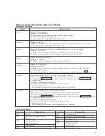
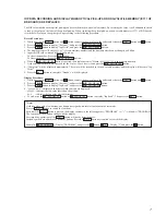
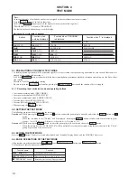
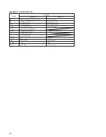
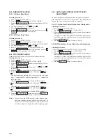
4-5. SELECTING THE TEST MODE

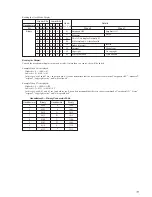
There are 27 types of test modes as shown below. The groups can be switched by pressing the  

=

  and  

=

  buttons. After selecting the

group to be used, press the  

^

 “PROGRAM”  button. After setting a certain group, pressing the   

=

  and  

=

  buttons switches between

these modes.
Refer to “Group” in the table for details selected.
All items used for servicing can be treated using group S. So be carefully not to enter other groups by mistake.

Display

TEMP CHECK

LDPWR CHECK

EF MO CHECK

EF CD CHECK

FBIAS CHECK

S curve CHECK

VERIFY MODE

DETRK CHECK

TEMP ADJUST

LDPWR ADJUST

EF MO ADJUST

EF CD ADJUST

FBIAS ADJUST

EEP MODE

MANUAL CMD

SVDATA READ

ERR DP MODE

SLED MOVE

Inpossible

ADJ CLEAR

AG Set (MO)

AG Set (CD)

Iop Read

Iop Write

INFORMATION

CPLAY MODE

CREC MODE

Contents

Temperature compensation offset check

Laser power check

Traverse (MO) check

Traverse (CD) check

Focus bias check

S letter check

Non-volatile memory check

Detrack check

Temperature compensation offset adjustment

Laser power adjustment

Traverse (MO) adjustment

Traverse (CD) adjustment

Focus bias adjustment

Non-volatile memory control

Command transmission

Status display

Error history display, clear

Sled check

No function

Initialization of non-volatile memory of adjustment value

Auto gain output level adjustment (MO)

Auto gain output level adjustment (CD)

IOP data display

IOP data write

Microprocessing version display

Continuous play mode

Continuous recording mode

Mark

(

X

)

(

X

)

(

X

)

(X

) (!)

(

X

)

(

X

)

(X

)

(

X

)

Group (

*

)

C

S

C

S

C

S

C

S

C

S

C

C

C

A

S

A

S

A

S

A

S

A

S

D

D

D

S

D

D

A

S

A

S

A

S

C

S

A

S

C

S

C

A

S

D

C

A

S

D

Group (

*

)

C: Check
S: Service

A: Adjust
D: Develop

• For details of each adjustment mode, refer to “5. Electrical Adjustments”.

For details of “ERR DP MODE”, refer to “Self-Diagnosis Function” on page 2.

• If a different mode has been selected by mistake, press the  

p

 “PROGRAM”  button to exit that mode.

• Modes with (

X

) in the Mark column are not used for servicing and therefore are not described in detail. If these modes are set accidentally,

press the  

p

 “PROGRAM”  button to exit the mode immediately. Be especially careful not to set the modes with (!) as they will overwrite

the non-volatile memory and reset it, and as a result, the unit will not operate normally.

Summary of Contents for MDS-PC2

Page 1: ... SPECIFICATIONS SERVICE MANUAL MINIDISC DECK Model Name Using Similar Mechanism MDS S40 MD Mechanism Type MDM 5A Optical Pick up Type KMS 260B J1N US Model Canadian Model AEP Model UK Model E Model Continued on next page ...

Page 2: ...when Service is displayed press the PROGRAM button 3 Press the button and display ERR DP MODE 4 Pressing the PROGRAM button sets the error history mode and displays total rec 5 Select the contents to be displayed or executed using the button 6 Pressing the r PROGRAM button will display or execute the contents selected 7 Pressing the r PROGRAM button another time returns to step 4 8 Pressing the p ...

Page 3: ...se the past error history After pressing the r PROGRAM button and er refresh is displayed press the PROGRAM button to erase the history Complete will be displayed momentarily Be sure to check the following when this mode has been executed The data has been erased The mechanism operates normally when recording and play are performed Mode which erases the total rec and total play histories These his...

Page 4: ... tilbage til leverandøren ADVARSEL Eksplosjonsfare ved feilakting skifte av batteri Benytt samme batteritype eller en tilsvarende type anbefalt av apparatfabrikanten Brukte batterier katterier kasseres i henhold til fabrikantens VARNIG Explosionsfara vid felaktigt batteribyte Använd samma batterityp eller en likvärdig typ som rekommenderas av apparattillverkaren Kassera använt batteri enligt gälla...

Page 5: ...ter correcting the original service problem perform the follow ing safety checks before releasing the set to the customer Check the antenna terminals metal trim metallized knobs screws and all other exposed metal parts for AC leakage Check leakage as described below LEAKAGE The AC leakage from any exposed metal part to earth Ground and from all exposed metal parts to any exposed metal part having ...

Page 6: ... Ground I 3V For measuring IOP Check the deterioration of the optical pick up laser IOP For measuring IOP Check the deterioration of the optical pick up laser TEO TRK error signal Traverse adjustment VC Reference level for checking the signal RF RF signal Check jitter RF VC TEO For MDM 3 For MDM 5 IOP I 3V VC RF TEO IOP I 3V GND VC RF TEO IOP I 3V GND 1 5 1 6 CN110 RF 5P connector 6P connector VC ...

Page 7: ... and press the PROGRAM button 8 Complete will be displayed momentarily The value will be recorded in the non volatile memory and the display will become Iop Write 9 Press the 6 1 button to complete Standby will be displayed Display Precedure 1 While pressing the INPUT button and p button connect the power plug to the outlet and release the INPUT button and p button 2 Press the button to display Se...

Page 8: ...eck disc TDYS 1 C1 error Below 50 CPLAY error rate check Specified value C1 error Below 80 AD error Below 2 Unsatisfactory if displayed as T NG NG are both arbitrary numbers Laser power check 5 6 2 See page 37 Traverse check 5 6 3 See page 37 Focus bias check 5 6 4 See page 38 C PLAY check 5 6 5 See page 38 Self recording playback check REC PLAY 5 6 6 See page 38 TEMP check Temperature compensatio...

Page 9: ...ing a remote commander end there and disconnect the power plug from the outlet If using a remote commander press any button 7 The check is completed when Chk End is displayed Press the I u button to end FORCED RESET The system microprocessor can be reset in the following procedure Use these procedure when the unit cannot be operated normally due to the overrunning of the microprocessor etc The lin...

Page 10: ...of the YES button for the same results 4 The fluorescent display tube displays RTs c e 5 Press the r button to start recording Then press the button and start recording 6 To check the track mode press the button to start play 7 To exit the test mode press the 1 u button If the test mode cannot be exited refer to Forced Reset on page 8 Address Physical address on disc Hexadecimal Bit Binary Higher ...

Page 11: ...mphasis ON stereo original copyright exists and write prohibited Hexadecimal n Binary Conversion Table Hexadecimal Binary Hexadecimal Binary 0 1 2 3 4 5 6 7 8 9 A B C D E F 0000 0001 0010 0011 0100 0101 0110 0111 1000 1001 1010 1011 1100 1101 1110 1111 Hexadecimal Bit Binary Higher Bits Lower Bits 8 4 2 1 8 4 2 1 b7 b6 b5 b4 b3 b2 b1 b0 0 0 0 0 0 0 0 1 0 0 0 0 0 0 1 0 0 0 0 0 0 1 0 0 0 0 0 0 1 0 0...

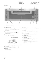
Page 12: ...12 This section is extracted from instruction manual Location of Parts and Controls SECTION 2 GENERAL Front Panel 2 4 6 7 8 9 10 11 1 3 5 ...

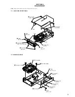
Page 13: ...of two claws 9 Flat type wire CN701 1 Two screws Flat head 2 Two screws Flat head 3 Case 4 Two screws BTT M3 6 Screw M2 x 6 0 7 Screw M2 x 6 0 5 Screw BTT M3 Claw Claw 8 Two step screws 7 Main board 6 Screw BVTP 3 x 8 5 Screw BVTP 3 x 8 1 Connector 8P CN503 2 Flat type wire CN412 3 Flat type wire CN501 4 Flat type wire CN421 9 Two step screws 0 MD mechanism ...

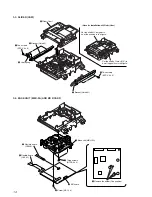
Page 14: ...6 4 Two screws BTP 2 6 x 6 Set the shaft of Lever O C to be at the position in the figure Set the shaft of Cam gear to be at the position in the figure Note for Installation of Slider Cam 4 Screw M1 7 x 4 1 Three screws BTP2 6 x 6 3 Remove the solder Five position 2 Base unit MBU 5A 6 Flexible board CN101 5 Flexible board CN104 7 BD board ...

Page 15: ...15 3 5 SW BOARD AND LOADING MOTOR M103 5 Three screws BTP2 6 x 6 4 Loading motor M103 6 SW board 2 Gear B 3 Two screws PWH 1 7 x 3 1 Screw PTPWH M2 6 x 6 ...

Page 16: ...t Nn Service Nn Develop Nn Procedure 2 While pressing the INPUT button connect the power plug to the outlet and release the INPUT button When the test mode is set TEMP CHECK will be displayed By setting the test mode using this procedure only the Check group of procedure 1 can be executed 4 3 EXITING THE TEST MODE Press the p 1 button The disc is ejected when loaded and Standby display blinks and ...

Page 17: ...justment Traverse MO adjustment Traverse CD adjustment Focus bias adjustment Non volatile memory control Command transmission Status display Error history display clear Sled check No function Initialization of non volatile memory of adjustment value Auto gain output level adjustment MO Auto gain output level adjustment CD IOP data display IOP data write Microprocessing version display Continuous p...

Page 18: ...s the button and display CREC MODE 3 Press the PROGRAM button to change the display to CREC MID 4 When access completes the display changes to CREC and REC lights up Note The numbers displayed shows you the recording position addresses 2 Changing the parts to be recorded 1 When the PROGRAM button is pressed during continuous recording the display changes as below When pressed another time the part...

Page 19: ...OGRAM The functions of each button change with the display Mode display Error rate display Address display Auto gain display Not used in servicing Detrack check display Not used in servicing IVR display Not used in servicing 4 7 TEST MODE DISPLAYS Each time the p 1 button is pressed the display changes in the following order 1 Mode display Displays TEMP ADJUST CPLAYMODE etc 2 Error rate display Di...

Page 20: ...ervo OFF Recording mode ON CLV low speed mode ABCD adjustment completed Tracking offset cancel ON Tracking auto gain OK Focus auto gain OK Pit High reflection CLV S CLV LOCK MEANINGS OF OTHER DISPLAYS STOP CLV OFF Tracking servo ON Recording mode OFF CLV normal mode Tracking offset cancel OFF Groove Low reflection CLV A CLV UNLOCK ...

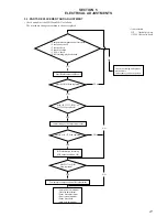
Page 21: ... playback check Parts Replacement and Repair NG Has the OWH been replaced NO OK NO NO NO Has OP IC171 IC101 or IC121 been replaced YES YES Initial setting of the adjustment value Has OP or IC171 been replaced YES IOP information recording IOP value labeled on OP Has IC171 or D101 been replaced YES Temperature compensation offset adjustment Laser power adjustment Traverse adjustment Focus bias adju...

Page 22: ...s No 4 963 646 01 Test Disk MDW 74 AU 1 Parts No 8 892 341 41 Laser power meter LPM 8001 Parts No J 2501 046 A or MD Laser power meter 8010S Parts No J 2501 145 A Oscilloscope Measure after performing CAL of prove Digital voltmeter Thermometer Jig for checking BD board waveform Parts No J 2501 149 A 5 When observing several signals on the oscilloscope etc make sure thatVC and ground do not connect...

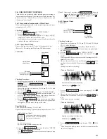
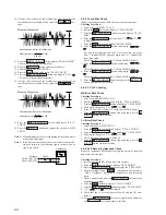
Page 23: ...and display LDPWR CHECK and stop the laser emission The p PROGRAM button is effective at all times to stop the laser emission 5 6 3 Traverse Check Connection Checking Procedure 1 Connect an oscilloscope to CN110 pin 3 TE and CN110 pin 1 VC of the BD board 2 Load a disc any available on the market Refer to Note 1 3 Press the PROGRAM button and move the optical pick up outside the pit 4 Press the bu...

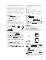
Page 24: ...disc using the unit to be repaired and check the error rate Checking Procedure 1 Insert a recordable disc blank disc into the unit 2 Press the button knob to display CREC MODE 3 Press the PROGRAM button to display the CREC MID 4 When recording starts REC is displayed this becomes CREC is the address and recording starts 5 About 1 minute later press the p PROGRAM button to stop continuous recording...

Page 25: ...layed indicates the Iop value labeled on the pick up indicates the Iop value after adjustment 3 To end press the r PROGRAM button or p PROGRAM button to display Iop Read 5 9 TEMPERATURE COMPENSATION OFFSET ADJUTMENT Save the temperature data at that time in the non volatile memory as 25 C reference data Note 1 Usually do not perform this adjustment 2 Perform this adjustment in an ambient temperatu...

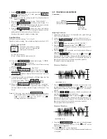
Page 26: ... Procedure 1 Connect an oscilloscope to CN110 pin 3 TE and CN110 pin 1 VC of the BD board 2 Load a disc any available on the market Refer to Note 1 3 Press the PROGRAM button and move the optical pick up outside the pit 4 Press the button and display EF MO ADJUST 5 Press the button and display EFB MO R Laser power READ power Focus servo ON tracking servo OFF spindle S servo ON 6 Press the button s...

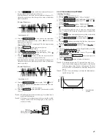
Page 27: ...hat it can be seen more clearly 5 12 FOCUS BIAS ADJUSTMENT Adjusting Procedure 1 Load a test disk MDW 74 AU 1 2 Press the button and display CPLAY MODE 3 Press the PROGRAM button and display CPLAY MID 4 Press the p PROGRAM button when C1 AD is displayed 5 Press the button and display FBIAS ADJUST 6 Press the p PROGRAM button and display a The first four digits indicate the C1 error rate the two di...

Page 28: ... below 220 and ADER is below 2 8 Press the PROGRAM button and display a Check that the C1 error is below 220 and ADER is below 2 9 Press the p PROGRAM button next press the 6 EJECT button and remove the continuously recorded disc Note 1 If the C1 error and ADER are above other than the speci fied value at points a step 8 in the above or b step 7 in the above the focus bias adjustment may not have ...

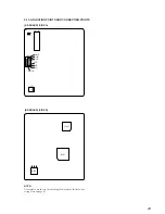
Page 29: ...l to use the jig for checking the waveform Refer to Ser vicing Note on page 6 5 15 ADJUSTING POINTS AND CONNECTING POINTS BD BOARD SIDE A BD BOARD SIDE B CN110 NOTE D101 I 3V IOP TE VC GND IC171 IC121 IC101 IC192 CN101 RF ...

Page 30: ...30 SECTION 6 DIAGRAMS 6 1 CIRCUIT BOARDS LOCATION Back up board SW board BD board Panel board Main board Power board ...

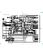
Page 31: ... DOUT 91 92 85 86 89 88 83 13 RECP APCREF FFDR FRDR TFDR TRDR SFDR SRDR FOCNT XLAT SCLK SWDT CSLED SE TE 26 28 32 30 ADFG ADIN ADFM 29 31 34 66 68 75 74 FE VC TE SE 33 67 36 37 35 64 63 65 AUX BOTM PEAK ABCD FE AUX1 BOTM PEAK ABCD 38 RF 57 RFI 59 60 61 62 ABCD AMP FOCUS ERROR AMP I J A B C D E F VC CVB TEMP AMP TEMPR TEMPI APC APCREF EQADJ 3TADJ WBLADJ TRACKING ERROR AMP OPTICAL PICK UP BLOCK KMS ...

Page 32: ...0 5 I 51 LD LOVO 9 10 2 4 7 X513 10MHz LD LOW SWITCH Q441 LED SW Q751 RECTIFIER D411 412 RECTIFIER D431 432 MUTE Q191 8 7 5 4 MUTE DRIVE Q390 GRID DRIVE Q767 FL701 FLUORESCENT INDICATOR TUBE STANDBY FL DRIVER IC761 IC611 IC601 A D D A CONVERTER IC301 LINE AMP IC381 382 IC601 IC351 IC351 SYSTEM CONTROL IC501 3 IC621 1 IC661 DATAO VINL1 VINR1 R CH R CH VOUTL VOUTR L3MODE L3CLK L3DATA BCK WS DATAI SY...

Page 33: ... parts mounted on the conductor side Through hole b Pattern from the side which enables seeing The other layers patterns are not indicated U B Line V B Line H adjustment for repair no mark STOP Play the test disk TDYS 1 REC Can not be measured Voltages are taken with aVOM Input impedance 10 MΩ Voltage variations may be noted due to normal produc tion tolerances Waveforms are taken with a oscillosc...

Page 34: ...01 A 1 D181 D 3 D183 D 3 IC103 B 1 IC123 D 2 IC171 D 1 Q102 B 1 Q103 B 1 Q104 B 1 SEMICONDUCTOR LOCATION Ref No Location IC101 A 3 IC121 C 3 IC124 C 3 IC152 B 1 IC181 C 1 IC192 D 1 Q101 B 3 Q162 B 3 Q163 B 3 Q181 C 1 Q182 C 2 SEMICONDUCTOR LOCATION Ref No Location SOLDER BRIDGE Page 43 Page 39 ...

Page 35: ...35 35 MDS PC2 6 4 SCHEMATIC DIAGRAM BD 1 2 SECTION See page 33 for Waveform See page 45 for IC Block Diagrams See page 48 for IC Pin Function Page 36 Page 36 Page 36 Page 36 Page 36 Page 36 Page 36 ...

Page 36: ...PC2 6 5 SCHEMATIC DIAGRAM BD 2 2 SECTION See page 33 for Waveform See page 34 for Printed Wiring Board Page 35 Page 35 Page 35 Page 35 Page 35 Page 35 Page 35 Page 37 Page 42 BA033FP E2 MAIN BOARD 1 2 POWER BOARD ...

Page 37: ... SCHEMATIC DIAGRAM MAIN 1 2 SECTION See page 33 for Waveform See page 39 for Printed Wiring Board Page 44 Page 36 Page 42 Page 38 Page 38 Page 38 Page 38 SW BOARD BD BOARD 2 2 POWER BOARD See page 51 for IC Pin Function ...

Page 38: ...38 38 MDS PC2 6 7 SCHEMATIC DIAGRAM MAIN 2 2 SECTION See page 33 for Waveform See page 47 for IC Block Diagrams Page 37 Page 37 Page 37 Page 37 Page 40 PANEL BOARD IN L R L R OUT LINE ANALOG ...

Page 39: ...on IN OUT L L R R LINE ANALOG SEMICONDUCTOR LOCATION D390 A 2 D391 A 2 IC301 A 3 IC308 A 1 IC351 A 4 IC381 A 2 IC382 A 2 IC441 A 5 IC501 B 7 Q191 A 1 Q192 A 1 Q291 A 1 Q292 A 1 Q390 A 2 Q441 B 6 Ref No Location Page 43 Page 44 Page 34 Page 41 POWER BOARD BD SWITCH BOARD BD BOARD PANEL BOARD ...

Page 40: ...40 40 MDS PC2 6 9 SCHEMATIC DIAGRAM PANEL SECTION See page 33 for Waveform Page 38 MAIN BOARD 2 2 ...

Page 41: ...41 41 MDS PC2 6 10 PRINTED WIRING BOARD PANEL SECTION See page 30 for Circuit Boards Location Page 39 MAIN BOARD ...

Page 42: ...42 42 MDS PC2 6 11 SCHEMATIC DIAGRAM POWER SECTION Page 37 Page 36 BD BOARD 2 2 MAIN BOARD 1 2 IN 1 IN 2 OUT DIGITAL OPTICAL RESET ...

Page 43: ... C 2 D466 B 2 D467 B 2 D801 E 1 IC601 C 1 Ref No Location SEMICONDUCTOR LOCATION D411 C 4 D412 C 3 D421 C 2 D422 C 1 D451 B 2 D452 B 2 D461 B 4 D462 B 4 D911 B 4 D912 C 2 Ref No Location IC411 B 2 IC421 C 1 IC611 C 5 IC621 B 5 IC661 D 5 Q801 E 5 Ref No Location Page 39 MAIN BOARD IN 1 IN 2 OUT DIGITAL OPTICAL CONTROL A1 II Page 34 BD BOARD ...

Page 44: ...37 PEAK 36 BOTM 35 ABCD 34 FE 33 AUX 32 ADFG 31 ADAGC 30 ADIN 29 ADFM 28 SE 27 CSLED 26 TE 25 WBLADJ 24 VCC 23 3TADJ 22 EQADJ 21 VREF 20 F0CNT 19 XSTBY 18 XLAT 17 SCLK 16 SWDT 15 TEMPR 14 TEMPI 13 GND 12 APCREF 11 APC 10 PD 9 F 8 E 7 D 6 C 5 B 4 A 3 VC VI CONV BGR VREF SCRI PARA DECODE AUXSW COMMAND IVR GSW IV FF FBAL FF TG SEA 1 2 TG TEA WBL 3T EQ DET ADIP AGC WBL BPF22 BPFC ABCDA FEA WBL ATA CVB...

Page 45: ...13 RECP 12 DQSY 11 SQSY 10 XRST 9 SENS 8 SRDT 7 XLAT 6 SCLK 5 SWDT 4 MNT3 3 MNT2 2 MNT1 1 MNT0 PWM GENERATOR AUTO SEQUENCER SERVO DSP CPU I F MONITOR CONTROL SPINDLE SERVO EACH BLOCK EACH BLOCK DIGITAL AUDIO I F SAMPLING RATE CONVERTER CLOCK GENERATOR SUBCODE PROCESSOR EACH BLOCK A D CONVERTER ANALOG MUX EFM ACIRC ENCODER DECODER APC PLL SHOCK RESISTANT MEMORY CONTROLLER ATRAC ENCODER DECODER DRAM...

Page 46: ...IXER DIGITAL AGC ADC1L ADC2L ADC2R ADC1R DAC DAC 0DB 6DB SWITCH VSS AD VDD AD VINL1 VDDD VSSD 18 16 19 17 26 25 27 24 13 15 14 9 22 10 11 23 28 12 20 21 DATAO BCK WS DATAI QMUTE VREF VOUTL VDD DAC VSS DAC VOUTR TEST2 TEST1 SYSCLK L3DATA L3MODE L3CLOCK OVERFLOW AGCSTAT VINR1 VINR2 IC301 UDA1341TS N2 1 LOGIC PREDRIVER VREF 2 3 4 5 10 9 8 7 6 IN2 IN1 VM VREF VCONT VCC OUT2 GND OUT1 VS IC441 LB1830M ...

Page 47: ...ernal circuit BPF22 Tracking error signal output to the CXD2650R or CXD2652AR External capacitor connection pin for the sled error signal LPF Sled error signal output to the CXD2650R or CXD2652AR FM signal output of ADIP ADIP signal comparator input ADFM is connected with AC coupling External capacitor connection pin for AGC of ADIP ADIP duplex signal output to the CXD2650R or CXD2652AR I3 signal ...

Page 48: ... from the system control L Reset Subcode Q sync SCOR output to the system control L is output every 13 3 msec Almost all H is output Digital In U bit CD format or MD format subcode Q sync SCOR output to the system control Laser power switching input from the system control H Recording L Playback Interrupt status output to the system control Recording data output enable input from the system contro...

Page 49: ...from the CXA2523R Light amount signal input from the CXA2523R Focus error signal input from the CXA2523R Auxiliary A D input Middle point voltage 1 5V input from the CXA2523R Monitor output of the A D converter input signal Not used 3V power supply Analog A D converter operational range upper limit voltage input Fixed at H A D converter operational range lower limit voltage input Fixed at L Ground...

Page 50: ...king servo drive PWM output 3V power supply Digital Focus servo drive PWM output Focus servo drive PWM output 176 4 kHz clock signal output X tal Not used Sled servo drive PWM output Sled servo drive PWM output Spindle servo drive PWM output Spindle servo drive PWM output Test input Fixed at L Ground Digital EFM output when recording Abbreviation EFM Eight to Fourteen Modulation ...

Page 51: ...1 Writing data signal output to the serial bus Reading data signal input from the serial bus Clock signal output to the serial bus Chip select signal output to the display driver Serial data signal output to the display driver Not used Fixed at L Serial clock signal output to the display driver Not used Not used Not used A1 output Not used Serial mode signal output to IC301 Not used Reset L DA lin...

Page 52: ...ction switch Protect H Disk reflection rate detection input from the reflect detection switch Disk with low reflection rate H Laser ON OFF control output H Laser ON Internal status SENSE input from the CXD2654R Track jump signal input from the CXD2654R Digital rest signal output to the CXD2654R and motor driver Reset L In the state of executive command from the CXD2654R Latch signal output to the ...

Page 53: ...8 11 WIRE FLAT TYPE 23 CORE 90mm 18 1 791 159 11 WIRE FLAT TYPE 21 CORE 19 4 220 570 11 PANEL BACK 20 3 703 244 00 BUSHING 2104 CORD 21 1 696 586 21 CORD POWER UK 21 1 751 275 11 CORD POWER AEP SP 21 1 783 531 31 CORD POWER US CND 22 3 703 249 01 SCREW S TIGHT PTTWH 3X6 23 4 965 822 01 FOOT 24 A 4724 780 A POWER BOARD COMPLETE US CND 24 A 4724 784 A POWER BOARD COMPLETE AEP UK SP 25 1 674 897 11 B...

Page 54: ...NG SHUTTER LEAF 526 A 4680 417 A HOLDER COMPLETE ASSY M103 X 4949 264 1 MOTOR ASSY LOADING 501 1 668 111 11 SW BOARD 502 4 996 217 01 CHASSIS 503 4 996 223 01 INSULATOR F 504 4 996 218 01 BRACKET GUIDE R 505 4 996 277 01 SPRING O C TENSION 506 4 996 226 01 LEVER O C 507 4 999 347 01 INSULATOR R 508 4 996 225 01 BRACKET GUIDE L 509 4 988 466 21 SPRING ELECTROSTATIC LEAF 510 4 996 219 01 GEAR CAM GE...

Page 55: ...1 BASE BU D 554 4 996 255 01 BASE BU C 555 4 900 590 01 SCREW PRECISION SMALL 556 4 996 258 01 SPRING COMPRESSION 557 4 996 262 01 GEAR SL C 558 1 667 954 11 FLEXIBLE BOARD 559 4 210 664 01 BASE BU A 560 A 4672 541 A OPTICAL PICK UP KMS 260B J1N 561 4 996 252 01 CHASSIS BU 562 4 996 254 01 BASE BU B 563 4 967 688 11 MAGNET ABSORPTION 564 4 996 260 01 GEAR SL A Les composants identifiés par une mar...

Page 56: ... CERAMIC CHIP 100PF 5 50V C131 1 163 023 00 CERAMIC CHIP 0 015uF 5 50V C132 1 107 823 11 CERAMIC CHIP 0 47uF 10 16V C133 1 163 017 00 CERAMIC CHIP 0 0047uF 5 50V C134 1 163 038 91 CERAMIC CHIP 0 1uF 25V C135 1 163 038 91 CERAMIC CHIP 0 1uF 25V C136 1 126 206 11 ELECT CHIP 100uF 20 6 3V C142 1 163 251 11 CERAMIC CHIP 100PF 5 50V C143 1 163 251 11 CERAMIC CHIP 100PF 5 50V C144 1 163 251 11 CERAMIC C...

Page 57: ... 216 117 00 METAL CHIP 680K 5 1 10W R134 1 216 049 91 RES CHIP 1K 5 1 10W R135 1 216 061 00 METAL CHIP 3 3K 5 1 10W R136 1 216 049 91 RES CHIP 1K 5 1 10W R137 1 216 295 91 SHORT 0 R140 1 216 029 00 METAL CHIP 150 5 1 10W R142 1 216 073 00 METAL CHIP 10K 5 1 10W R143 1 216 073 00 METAL CHIP 10K 5 1 10W R144 1 216 025 91 RES CHIP 100 5 1 10W R145 1 216 073 00 METAL CHIP 10K 5 1 10W R146 1 216 037 00...

Page 58: ...0V C597 1 163 009 11 CERAMIC CHIP 0 001uF 10 50V C598 1 163 038 91 CERAMIC CHIP 0 1uF 25V C599 1 163 038 91 CERAMIC CHIP 0 1uF 25V C951 1 104 664 11 ELECT 47uF 20 10V C953 1 163 038 91 CERAMIC CHIP 0 1uF 25V C954 1 163 038 91 CERAMIC CHIP 0 1uF 25V CONNECTOR CN412 1 784 834 21 CONNECTOR FFC LIF NON ZIF 23P CN421 1 793 448 11 CONNECTOR FFC 15P CN501 1 784 834 21 CONNECTOR FFC LIF NON ZIF 23P CN502 ...

Page 59: ...P 10K 5 1 10W R581 1 216 097 91 RES CHIP 100K 5 1 10W R595 1 216 073 00 METAL CHIP 10K 5 1 10W R597 1 216 073 00 METAL CHIP 10K 5 1 10W R852 1 216 097 91 RES CHIP 100K 5 1 10W VIBRATOR X351 1 579 314 11 VIBRATOR CRYSTAL 22 5792MHz X513 1 781 174 21 VIBRATOR CERAMIC 10MHz A 4724 778 A PANEL BOARD COMPLETE US CND A 4724 786 A PANEL BOARD COMPLETE AEP UK SP 4 220 557 01 HOLDER FL 4 949 935 51 CUSHION...

Page 60: ...35 00 METAL CHIP 270 5 1 10W R434 1 216 081 00 METAL CHIP 22K 5 1 10W R435 1 216 091 00 METAL CHIP 56K 5 1 10W R436 1 216 109 00 METAL CHIP 330K 5 1 10W R437 1 216 049 91 RES CHIP 1K 5 1 10W R451 1 216 033 00 METAL CHIP 220 5 1 10W R613 1 216 113 00 METAL CHIP 470K 5 1 10W R614 1 216 089 91 RES CHIP 47K 5 1 10W R623 1 216 113 00 METAL CHIP 470K 5 1 10W R624 1 216 089 91 RES CHIP 47K 5 1 10W R801 1...

Page 61: ...RE FLAT TYPE 23 CORE 90mm 18 1 791 159 11 WIRE FLAT TYPE 21 CORE 21 1 696 586 21 CORD POWER UK 21 1 751 275 11 CORD POWER AEP SP 21 1 783 531 11 CORD POWER US CND 27 1 569 008 21 ADAPTOR CONVERSION 2P SP 558 1 667 954 11 FLEXIBLE BOARD 560 A 4672 541 A OPTICAL PICK UP KMS 260B J1N FL701 1 517 907 11 INDICATOR TUBE FLUORESCENT HR901 1 500 502 11 HEAD OVER LIGHT M101 A 4672 475 A MOTOR ASSY SPINDLE ...

Page 62: ...62 Sony Corporation Home Audio Company 9 928 916 11 SP 99F0986 1 Printed in Japan 1999 6 Published by Quality Assurance Dept MDS PC2 ...

Reviews: