— 98 —
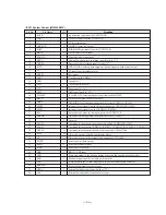
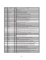
48, 49
50
51
52 to 55
56 to 60
61
62
63
64
65
66
67
68, 69
70, 71
72 to 74
75
76
77
78
79
80
81
82
83
84
85
86
87
88
89
90
91
92
93
94
95
96
97
98
99
100
A11, A10
VSS
VDD
A03 to A00
A04 to A08
XOE
XCAS
VSS
XCS
A09
XRAS
XWE
D1, D0
D2, D3
D4 to D6
VSS
D7
ERR
EXTC2R
BUSY
EMP
FUL
EQL
MDLK
CPSY
CTMD0
CTMD1
SPO
VSS
MDSY
LRCK
BCK
C2PO
DATA
DIDT
DODT
DIRCPB
MIN
SPOSL
MCK
VSS
O
—
—
O
O
O
O
—
O
O
O
O
I/O
I/O
I/O
—
I/O
I/O
I
O
O
O
O
O
O
O
O
I
—
O
I
I
I
I/O
I
O
O
I
I
O
—
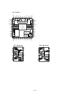
Address signal output (Not used)
Ground
Power supply (+5V)
Output of address signal to RAM (IC408)
Output of address signal to RAM (IC408)
Output of output enable control signal to RAM (IC408)
Output of column address strobe signal to RAM (IC408)
Ground
Output of chip select signal to RAM (IC408) (Not used)
Output of address signal to RAM (IC408)
Output of row address strobe signal to RAM (IC408)
Output of read/write control signal to RAM (IC408)
Input/output of data signal to/from RAM (IC408)
Data signal input/output (Not used)
Ground
Data signal input/output (Not used)
Input/output of error (C2PO) data to external RAM (Not used)
External RAM selection input for error data writing (“H”: External RAM) (Fixed at “L”)
RAM access BUSY signal output (Not used)
EMPTY or immediately before FULL of ATRAC data (When DSC=ASC+1: “H”)
(Not used)
FULL or immediately before EMPTY of ATRAC data (When ASC=DSC+1: “H”)
(Not used)
ATRAC data EMPTY (When DSC=ASC: “H”) (Not used)
Indicates recording/playback data main/sub (“H”: Sub, Linking: “L”: Main) (Not used)
Interpolation sync signal output (Not used)
DSC counter mode output (Not used)
Input of system clock (512fs) signal from CXD2536CR (IC401)
Ground
Main data sync detection signal output (Not used)
Input of L/R clock signal from CXD2535CR (IC121) (44.1 kHz)
Input of bit clock signal from CXD2535CR (IC121) (2.8224 MHz)
Input of C2PO signal from CXD2535CR (IC121) (Shows data error status)
Playback:C2PO (“H”). Digital recording: D.In-Vflag. Analog recording: “L”
Recording:Output of recording audio data signal to CXD2535CR (IC121)
Playback:Input of playback audio data signal from CXD2535CR (IC121)
Input of digital audio input data (Not used)
Output of digital audio output data (Not used)
Disc drive and EFM encoder/decoder recording/playback mode output (Not used)
Input of defect ON/OFF switching signal (Fixed at “L”)
Pin 87 (SPO) input/output switching input (“L”:IN. “H”:OUT) (Fixed at “L”)
RAM controller internal master clock output (Not used)
Ground
Function
Pin No.
Pin Name
I/O
Summary of Contents for MDS-B5
Page 2: ... 2 ...
Page 5: ... 5 SECTION 1 GENERAL This section is extracted from instruction manual ...
Page 6: ... 6 ...
Page 7: ... 7 ...
Page 8: ... 8 ...
Page 9: ... 9 ...
Page 10: ... 10 ...
Page 11: ... 11 ...
Page 12: ... 12 ...
Page 13: ... 13 ...
Page 14: ... 14 ...
Page 15: ... 15 ...
Page 16: ... 16 ...
Page 17: ... 17 ...
Page 18: ... 18 ...
Page 19: ... 19 ...
Page 20: ... 20 ...
Page 21: ... 21 ...
Page 22: ... 22 ...
Page 23: ... 23 ...
Page 24: ... 24 ...
Page 25: ... 25 ...
Page 26: ... 26 ...
Page 27: ... 27 ...
Page 28: ... 28 ...
Page 29: ... 29 ...
Page 30: ... 30 ...
Page 31: ... 31 ...
Page 32: ... 32 ...
Page 49: ......
Page 50: ......
Page 51: ......
Page 52: ......
Page 53: ......
Page 54: ......
Page 55: ......
Page 56: ......
Page 57: ......
Page 58: ......


