background image

– 4 –

SECTION 3

DISASSEMBLY

Note :

 Follow the disassembly procedure in the numerical order given.

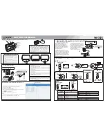
3-1. UPPER PANEL ASSY

r

 The equipment can be removed using the following procedure.

3-2. MECHANISM DECK SECTION

set

Main board, Audio board

Switch board

Mechanism deck section

Optical pick-up block ASSY

Upper panel ASSY

4

 Screw  (M1.4) step

5

 Screws  (M1.4) precision pan

3

7

1

2

6

OPEN knob

Upper panel ASSY

Lid, Battery case

Main unit

1

 Screws  (M1.4) precision pan

3

 CLV flexible board

4

 Flexible

   board

Main unit

Main board

Slider ASSY, Open

Mechanism deck section

2

5

Summary of Contents for MD Walkman MZ-E55

Page 1: ...se 20 to 20 000 Hz 3 dB Wow and Flutter Below measurable limit Outputs Headphones stereo mini jack maximum output level 5mW 5mW load impedance 16 ohm General Power requirements Rechageable battery supplied Nickel metal hydride rechargeable battery NH 9WM N One LR6 size AA alkaline battery not supplied Sony AC Power Adaptor not supplied connected at the DC IN 1 5V jack Battery operation time Batter...

Page 2: ...side of a tantalum capacitor may be dam aged by heat TABLE OF CONTENTS CAUTION Use of controls or adjustments or performance of procedures other than those specified herein may result in hazardous radiation exposure IN NO EVENT SHALL SELLER BE LIABLE FOR ANY DIRECT INCIDENTAL OR CONSEQUENTIAL DAMAGES OF ANY NATURE OR LOSSES OR EXPENSES RESULTING FROM ANY DEFECTIVE PRODUCT OR THE USE OF ANY PRODUCT...

Page 3: ...LSs witc h 5 Batterycompartment 6 VOLUME b uttons 7 MDoperateb uttons FF PLA Y REW p STOP 8 Externalbatteryterminal 9 OPENknob º2 REMOTE jac k 1 Headphones 2 MDoperateswitchandbuttons PLAY FF REW p STOP 3 VOL button 4 Displa ywindo w 5 DISPLAYbutton 6 PLAYMODEbutton 7 P PAUSE b utton 8 HOLD cswitch 9 p STOP b utton 2 7 3 1 6 4 º 9 5 8 1 2 3 4 5 6 8 9 7 ...

Page 4: ... 3 2 MECHANISM DECK SECTION set Main board Audio board Switch board Mechanism deck section Optical pick up block ASSY Upper panel ASSY 4 Screw M1 4 step 5 Screws M1 4 precision pan 3 7 1 2 6 OPEN knob Upper panel ASSY Lid Battery case Main unit 1 Screws M1 4 precision pan 3 CLV flexible board 4 Flexible board Main unit Main board Slider ASSY Open Mechanism deck section 2 5 ...

Page 5: ...crews M1 4 step Claw 2 3 Main board Switch board Switch flexible board Label Caution Case Battery 1 Screw NOTE When removing the audio board lift up on the board so that the connector separates vertically NOTE The caution label 4 213 092 01 affixed to the switch flexible board will be damaged or deformed when the switch board or the switch flexible board is removed so replace it with a new caution...

Page 6: ... 6 3 5 OPTICAL PICK UP BLOCK ASSY 1 4 5 3 Optical pick up block ASSY Chassis ASSY Double sided adhesive tape Shaft Main Flexible board Flexible board 2 Screw M1 4 precision pan ...

Page 7: ...EST MODE on the main board Operation of Setting on Test Mode When the test mode is set the LCD displays the following The cycle the above ROM version display nAll lit n All off is repeated The ROM version is constantly displayed When the PLAY MODE key is pressed and hold down the dis play at that time is held so that display can be checked Configuration of Test Mode The test mode has the configura...

Page 8: ...on CD tracking gain 046 Lower reflection CD RF offset 047 Lower reflection CD RF gain 048 Lower reflection CD focus bias 050 CD adjustment Mode Description 051 CD EF balance 052 CD EF gain 053 CD ABCD gain 054 CD focus gain 055 CD tracking gain 056 CD RF offset 057 CD RF gain 058 CD focus bias See page 7 p key p key p key p key keys MO adjustment 0 3 0 031 to 039 1 key p key p key keys CD adjustme...

Page 9: ...frequency characteristics When the VOLUME keys is pressed in any mode the vol ume of the headphones is changed increased decreased in units of one step When the keys is pressed the volume of the headphones is maximized minimized For the volume value any changed value remains as it is basi cally However when the volume is switched from 114 to 115 or 118 to 119 it returns the default value Audio mod...

Page 10: ...nter over all adjustment mode When entering another mode refer to the configuration of test mode When the overall adjustment mode is entered the LCD on the remote commander display the following 1 Structure of Overall Adjustment Mode 040 Auto Power mode 3 0 0 UNREG check 31 0 Power OFF 3 1 1 p key p key key key key Start CD automatic adjustment MO automatic adjustment OK NG OK NG Overall adjustmen...

Page 11: ...D EF gain 41 041 Low reflection CD EF balance 42 043 Low reflection CD ABCD gain 43 044 Low reflection CD focus gain 44 045 Low reflection CD tracking gain 45 046 Low reflection CD RF offset 46 047 Low reflection CD RF gain SECTION 5 ELECTRICAL ADJUSTMENTS Notes for Adjustment In this set automatic adjustment of CD and MO can be per formed by entering the test mode Adjustments are performed in the...

Page 12: ... 1 When each adjustment mode is set according to the structure of servo mode the lower two digits of the mode No and the ad justment value written in EEPROM are displayed and lit on the LCD on the remote commander 2 When the P key is pressed the following display appears and the automatic adjustment is performed Note Although the VOLUME keys can be used to change the adjustment value to any value ...

Page 13: ...SW I Set AVLS switch input 27 DSP SINT I Interrupt input from DSP 28 DBB 0 I DIGITAL MEGA BASS switch input MID 29 DBB 1 I DIGITAL MEGA BASS switch input MAX 30 OPR LED O LED drive output 31 XWK CLR O Power IC wakeup factor latch clear output and motor driver IC control signal outpt 32 ADJUST I Normally Test mode select input L Test mode 33 SLEEP O Power supply circuit OFF signal output 34 SBUS CL...

Page 14: ...ation 63 66 Not used Open 67 SLD V CON O Sled servo outer voltage control output 68 SLC TR ON O Baypass transistor control output for sled drive power supply 69 HP MUTE O Headphone amplifier mute output 70 HP STBY O Headphone amplifier standby output 71 RMC SEL O TSB SSB selection signal output to remote commander terminal Not used Open 72 NV D0 O Serial data signal output for NVRAM 73 NV D1 I Ser...

Page 15: ... 15 17 16 MZ E55 Signal path J PLAY 6 2 BLOCK DIAGRAM ...

Page 16: ...olytics and tantalums All resistors are in Ω and 1 4 W or less unless otherwise specified Note The components identified by mark or dotted line with mark are critical for safety Replace only with part number specified A B Line Power voltage is dc 1 5V and fed with regulated dc power supply from battery terminal Voltages and waveforms are dc with respect to ground under no signal conditions no mark...

Page 17: ...PLL EFM PLL SUBQ ADIP DECODER EFM ACIRC DECODER SECTOR DECODER SSB CONTROL MONITOR I O etc DRAM PERIPHERAL CONTROL ADDRESS GENERATOR AC WDCK S DATA 8 8 16 16 8 8 12 10 CLOCK GENERATOR ATRAC DECODER FLAG AC LRCK AC WDCK AC BYCK AC DATA EFM DATA A B ECC DATA EBA WR REQ etc RD DT ECC ATDT XATWE DREQ XBUSY 5 8 8 SBD SBA SBW SBR SQREQ 2nd MSB EFM PLCK 3 4 8 VDD ADC VREF FE ABCD TE VRT1 RF VRT2 ADIP VRT...

Page 18: ... POWER SW PRE DRIVER STEP UP DOWN PRE DRIVER STEP UP PRE DRIVER PRE DRIVER 3 PHASE CONTROL PRE DRIVER PWM DRIVER PRE DRIVER PWM DRIVER VC VC VG VC VC VG VC VC VG VC VC VG VC VC VG VC VC VG VC VC VG VC VG VG VG VG VG VC VC VC VC REN ROE 1ntSTB 1ntSTB 1ntOE DO or DI F12 R12 F11 R11 R13 F13 R14 F14 OE VREG VREG CONT CLPF RGND VC GND VG PWM DI DO VB1 VB1 VB VB VB2 LI LI UO VO WO V0 V0 L2H L2L GND DCC2...

Page 19: ... 4 6 7 8 1 VCC PE NC GND CS SK DI DO 21 22 23 24 25 26 27 28 29 30 2 3 5 4 6 7 8 9 10 1 11 12 13 14 15 16 17 18 19 20 31 32 33 34 35 36 GND VRMC VREF INM RF DTC CRST XRST VBMON VC SPCKI SPCKO C2L C1L VB C1H C2H VG BAND GAP REFERENCE RESET VB SELECT SPCK BUFF CHARGE PUMP VSTB VBH SYSTEM CONTROL OSC1 STEP UP DC DC CONVERTER PWM1 MODE SELECT SAW OSC2 XWK1 XWK2 XWK3 XWK4 FFCLR SLEEP VBSEL CLK VB2 VB1 ...

Page 20: ...LD 8 4 212 883 11 KNOB HOLD BLUE HK 9 4 212 882 01 KNOB MB GOLD 9 4 212 882 11 KNOB MB BLUE HK 10 4 213 653 11 KNOB AVLS BLUE HK 10 4 213 653 01 KNOB AVLS GOLD 11 4 212 895 01 TERMINAL BOARD MINUS 12 4 963 883 21 SCREW M1 4 PRECISION PAN GOLD 12 4 963 883 31 SCREW M1 4 PRECISION PAN BLUE HK 13 4 963 883 21 SCREW M1 4 PRECISION PAN 14 X 4950 413 1 PLATE L ASSY FULCRUM 15 X 4950 578 1 UPPER PANEL AS...

Page 21: ...RING THRUST 63 X 4949 164 1 OPTICAL PICK UP BLOCK ASSY 64 4 214 478 01 SHAFT MAIN M901 8 835 594 02 MOTOR DC SPINDLE M902 1 698 764 21 MOTOR SLED SLED INCLUDING GEAR R1001 1 216 789 11 METAL CHIP 2 2 5 1 16W NEW TYPE The components identified by mark or dotted line with mark are critical for safety Replace only with part number specified 7 2 MECHANISM DECK SECTION MT MZE55 150 M902 M901 NEW TYPE R...

Page 22: ... 11 CERAMIC CHIP 0 1uF 25V C311 1 117 919 11 TANTAL CHIP 10uF 20 6 3V C312 1 117 919 11 TANTAL CHIP 10uF 20 6 3V C313 1 164 156 11 CERAMIC CHIP 0 1uF 25V C315 1 115 156 11 CERAMIC CHIP 1uF 10V C316 1 127 574 91 TANTAL CHIP 22uF 20 6 3V C501 1 107 826 11 CERAMIC CHIP 0 1uF 10 16V C502 1 117 720 11 CERAMIC CHIP 4 7uF 10V C503 1 164 227 11 CERAMIC CHIP 0 022uF 10 25V C504 1 162 962 11 CERAMIC CHIP 47...

Page 23: ...006 31 INDUCTOR CHIP 10uH L551 1 412 031 11 INDUCTOR CHIP 47uH L552 1 412 031 11 INDUCTOR CHIP 47uH L553 1 412 030 11 INDUCTOR CHIP 22uH L554 1 412 030 11 INDUCTOR CHIP 22uH L555 1 412 031 11 INDUCTOR CHIP 47uH L556 1 414 410 21 INDUCTOR 10uH L901 1 412 032 11 INDUCTOR CHIP 100uH L902 1 416 668 11 COIL CHOKE 10uH L903 1 414 410 21 INDUCTOR 10uH TRANSISTOR Q501 8 729 922 10 TRANSISTOR 2SA1577 QR Q5...

Page 24: ... 708 11 SWITCH FLEXIBLE BOARD 53 1 670 707 11 CLV FLEXIBLE BOARD 63 X 4949 164 1 OPTICAL PICK UP BLOCK ASSY M901 8 835 594 02 MOTOR DC SPINDLE M902 1 698 764 21 MOTOR SLED SLED INCLUDING GEAR R1001 1 216 789 11 METAL CHIP 2 2 5 1 16W NEW TYPE Note Use R1001 only with Ver 3 of microprocessor IC801 Using R1001 with other microprocessor versions will cause operating errors so be sure to remove it You...

Page 25: ... 34 MZ E55 9 924 958 11 Sony Corporation Personal A V Products Company 98J027017 1 Printed in Singapore 1998 10 Published by Quality Engineering Dept Shibaura ...

Page 26: ...el AEP Model UK Model E Model Tourist Model Model Name Using Similar Mechanism NEW MD Mechanism Type MT MZE55 150 Optical Pick up Mechanism Type ODX 1A 1B US and foreign patents licensed from Dolby Laboratories Licensing Corporation Design and specifications are subject to change without notice ...

Page 27: ...side of a tantalum capacitor may be dam aged by heat TABLE OF CONTENTS CAUTION Use of controls or adjustments or performance of procedures other than those specified herein may result in hazardous radiation exposure IN NO EVENT SHALL SELLER BE LIABLE FOR ANY DIRECT INCIDENTAL OR CONSEQUENTIAL DAMAGES OF ANY NATURE OR LOSSES OR EXPENSES RESULTING FROM ANY DEFECTIVE PRODUCT OR THE USE OF ANY PRODUCT...

Page 28: ...LSs witc h 5 Batterycompartment 6 VOLUME b uttons 7 MDoperateb uttons FF PLA Y REW p STOP 8 Externalbatteryterminal 9 OPENknob º2 REMOTE jac k 1 Headphones 2 MDoperateswitchandbuttons PLAY FF REW p STOP 3 VOL button 4 Displa ywindo w 5 DISPLAYbutton 6 PLAYMODEbutton 7 P PAUSE b utton 8 HOLD cswitch 9 p STOP b utton 2 7 3 1 6 4 º 9 5 8 1 2 3 4 5 6 8 9 7 ...

Page 29: ... 3 2 MECHANISM DECK SECTION set Main board Audio board Switch board Mechanism deck section Optical pick up block ASSY Upper panel ASSY 4 Screw M1 4 step 5 Screws M1 4 precision pan 3 7 1 2 6 OPEN knob Upper panel ASSY Lid Battery case Main unit 1 Screws M1 4 precision pan 3 CLV flexible board 4 Flexible board Main unit Main board Slider ASSY Open Mechanism deck section 2 5 ...

Page 30: ...crews M1 4 step Claw 2 3 Main board Switch board Switch flexible board Label Caution Case Battery 1 Screw NOTE When removing the audio board lift up on the board so that the connector separates vertically NOTE The caution label 4 213 092 01 affixed to the switch flexible board will be damaged or deformed when the switch board or the switch flexible board is removed so replace it with a new caution...

Page 31: ... 6 3 5 OPTICAL PICK UP BLOCK ASSY 1 4 5 3 Optical pick up block ASSY Chassis ASSY Double sided adhesive tape Shaft Main Flexible board Flexible board 2 Screw M1 4 precision pan ...

Page 32: ...EST MODE on the main board Operation of Setting on Test Mode When the test mode is set the LCD displays the following The cycle the above ROM version display nAll lit n All off is repeated The ROM version is constantly displayed When the PLAY MODE key is pressed and hold down the dis play at that time is held so that display can be checked Configuration of Test Mode The test mode has the configura...

Page 33: ...on CD tracking gain 046 Lower reflection CD RF offset 047 Lower reflection CD RF gain 048 Lower reflection CD focus bias 050 CD adjustment Mode Description 051 CD EF balance 052 CD EF gain 053 CD ABCD gain 054 CD focus gain 055 CD tracking gain 056 CD RF offset 057 CD RF gain 058 CD focus bias See page 7 p key p key p key p key keys MO adjustment 0 3 0 031 to 039 1 key p key p key keys CD adjustme...

Page 34: ...frequency characteristics When the VOLUME keys is pressed in any mode the vol ume of the headphones is changed increased decreased in units of one step When the keys is pressed the volume of the headphones is maximized minimized For the volume value any changed value remains as it is basi cally However when the volume is switched from 114 to 115 or 118 to 119 it returns the default value Audio mod...

Page 35: ...nter over all adjustment mode When entering another mode refer to the configuration of test mode When the overall adjustment mode is entered the LCD on the remote commander display the following 1 Structure of Overall Adjustment Mode 040 Auto Power mode 3 0 0 UNREG check 31 0 Power OFF 3 1 1 p key p key key key key Start CD automatic adjustment MO automatic adjustment OK NG OK NG Overall adjustmen...

Page 36: ...D EF gain 41 041 Low reflection CD EF balance 42 043 Low reflection CD ABCD gain 43 044 Low reflection CD focus gain 44 045 Low reflection CD tracking gain 45 046 Low reflection CD RF offset 46 047 Low reflection CD RF gain SECTION 5 ELECTRICAL ADJUSTMENTS Notes for Adjustment In this set automatic adjustment of CD and MO can be per formed by entering the test mode Adjustments are performed in the...

Page 37: ... 1 When each adjustment mode is set according to the structure of servo mode the lower two digits of the mode No and the ad justment value written in EEPROM are displayed and lit on the LCD on the remote commander 2 When the P key is pressed the following display appears and the automatic adjustment is performed Note Although the VOLUME keys can be used to change the adjustment value to any value ...

Page 38: ... AVLS switch input 27 DSP SINT I Interrupt input from DSP 28 DBB 0 I DIGITAL MEGA BASS switch input MID 29 DBB 1 I DIGITAL MEGA BASS switch input MAX 30 OPR LED O LED drive output 31 XWK CLR O Power IC wakeup factor latch clear output and motor driver IC control signal outpt 32 ADJUST I Normally Test mode select input L Test mode 33 SLEEP O Power supply circuit OFF signal output 34 SBUS CLK O SBB ...

Page 39: ...ation 63 66 Not used Open 67 SLD V CON O Sled servo outer voltage control output 68 SLC TR ON O Baypass transistor control output for sled drive power supply 69 HP MUTE O Headphone amplifier mute output 70 HP STBY O Headphone amplifier standby output 71 RMC SEL O TSB SSB selection signal output to remote commander terminal Not used Open 72 NV D0 O Serial data signal output for NVRAM 73 NV D1 I Ser...

Page 40: ... 15 17 16 MZ E55 Signal path J PLAY 6 2 BLOCK DIAGRAM ...

Page 41: ...lytics and tantalums All resistors are in Ω and 1 4 W or less unless otherwise specified Note The components identified by mark or dotted line with mark are critical for safety Replace only with part number specified A B Line Power voltage is dc 1 5V and fed with regulated dc power supply from battery terminal Voltages and waveforms are dc with respect to ground under no signal conditions no mark ...

Page 42: ... the original one Color indication of Appearance Parts Example KNOB BALANCE WHITE RED Parts color Cabinet s color Items marked are not stocked since they are seldom required for routine service Some delay should be anticipated when ordering these items The mechanical parts with no reference number in the exploded views are not supplied Accessories and packing materials are given in the last of thi...

Page 43: ...4 156 11 CERAMIC CHIP 0 1uF 25V C311 1 117 919 11 TANTAL CHIP 10uF 20 6 3V C312 1 117 919 11 TANTAL CHIP 10uF 20 6 3V C313 1 164 156 11 CERAMIC CHIP 0 1uF 25V C315 1 115 156 11 CERAMIC CHIP 1uF 10V C316 1 127 574 91 TANTAL CHIP 22uF 20 6 3V C501 1 107 826 11 CERAMIC CHIP 0 1uF 10 16V C502 1 117 720 11 CERAMIC CHIP 4 7uF 10V C503 1 164 227 11 CERAMIC CHIP 0 022uF 10 25V C504 1 162 962 11 CERAMIC CH...

Page 44: ...1 8 759 573 84 IC RU6815MF 0005 VERSION 3 2 IC801 8 759 580 35 IC RU6815MF 0006 VERSION 3 3 IC802 8 759 449 23 IC AK93C55AV L IC901 8 759 538 57 IC MPC1830ADTB JACK J301 1 779 867 61 JACK 2 REMOTE COIL L501 1 412 006 31 INDUCTOR CHIP 10uH L551 1 412 031 11 INDUCTOR CHIP 47uH L552 1 412 031 11 INDUCTOR CHIP 47uH L553 1 412 030 11 INDUCTOR CHIP 22uH L554 1 412 030 11 INDUCTOR CHIP 22uH L555 1 412 03...

Page 45: ...CH FLEXIBLE BOARD 53 1 670 707 11 CLV FLEXIBLE BOARD 63 X 4949 164 1 OPTICAL PICK UP BLOCK ASSY M901 8 835 594 02 MOTOR DC SPINDLE M902 1 698 764 21 MOTOR SLED SLED INCLUDING GEAR R1001 1 216 789 11 METAL CHIP 2 2 5 1 16W ACCESSORIES PACKING MATERIALS 1 475 831 22 REMOTE CONTROL UNIT RM MZE55 GOLD 1 475 831 52 REMOTE CONTROL UNIT RM MZE55 BLUE HK 1 528 580 21 BATTERY CHARGER BC 7HT Tourist 1 528 7...
Page 46: ... 34 MZ E55 9 924 958 12 Sony Corporation Personal A V Products Company 99A0288 1 Printed in Japan 1999 1 Published by Quality Engineering Dept Shibaura ...

Reviews: