


SERVICE MANUAL
Sony Corporation
Published by Sony Techno Create Corporation
SPECIFICATIONS
HOME AUDIO DOCKING SYSTEM
9-893-451-01
2012C33-1
©
2012.03
US Model
RDH-GTK33iP
AEP Model
UK Model
Saudi Arabia Model
Singapore Model
Malaysia Model
RDH-GTK11iP
E Model
FST-GTK11iP/GTK33iP
Australian Model
RDH-GTK11iP/GTK33iP
Chilean Model
Peruvian Model
FST-GTK33iP
Ver. 1.0 2012.03
FST-GTK11iP/GTK33iP/
RDH-GTK11iP/GTK33iP
License and Trademark Notice
iPhone, iPod, iPod classic, iPod nano, and iPod touch
are trademarks of Apple Inc., registered in the U.S. and
other countries.
MPEG Layer-3 audio coding technology and patents
licensed from Fraunhofer IIS and Thomson.
Windows Media is either a registered trademark or
trademark of Microsoft Corporation in the United
States and/or other countries.
This product contains technology subject to certain
intellectual property rights of Microsoft. Use or
distribution of this technology outside of this product
is prohibited without the appropriate license(s) from
Microsoft.
All other trademarks and registered trademarks are of
their respective holders. In this manual,
™
and
®
marks
are not specified.
Amplifier section (Except US model)
The following are measured at AC 120 V 240 V, 50/60 Hz (Latin American
models (except for Mexican and Argentine models))
The following are measured at AC 127 V, 60 Hz (Mexican model)
The following are measured at AC 220 V 240 V, 50/60 Hz (European,
Russian, Australian and Argentine models)
The following are measured at AC 120 V 240 V, 50/60 Hz (Other models)
FST-GTK33iP/RDH-GTK33iP
Power output (rated):
100 W + 100 W (at 3.5 Ω, 1 kHz, 1% THD)
RMS output power (reference):
210 W + 210 W (per channel at 3.5 Ω, 1 kHz)
FST-GTK11iP/RDH-GTK11iP
Power output (rated):
55 W + 55 W (at 3 Ω, 1 kHz, 1% THD)
RMS output power (reference):
115 W + 115 W (per channel at 3 Ω, 1 kHz)
Speaker section
Speaker system: 2 way speaker system, Bass reflex
Speaker units:
FST-GTK33iP/RDH-GTK33iP:
Woofer: 200 mm, cone type
Tweeter: 66 mm, cone type
FST-GTK11iP/RDH-GTK11iP:
Woofer: 160 mm, cone type
Tweeter: 40 mm, cone type
Rated impedance:
FST-GTK33iP/RDH-GTK33iP: 3.5 Ω
FST-GTK11iP/RDH-GTK11iP: 3.0 Ω
Input
DVD/PC IN (audio in L/R):
FST-GTK33iP/RDH-GTK33iP: Sensitivity 1,000 mV, impedance 47 kΩ
FST-GTK11iP/RDH-GTK11iP: Sensitivity 1,500 mV, impedance 47 kΩ
iPod/iPhone section
iPod/iPhone connector:
Output voltage: DC 5 V
Maximum output current: 1 A
Compatible iPod/iPhone models:
iPod touch 4th generation
iPod touch 3rd generation
iPod touch 2nd generation
iPod nano 6th generation
iPod nano 5th generation (video camera)
iPod nano 4th generation (video)
iPod nano 3rd generation (video)
iPod classic
iPhone 4S
iPhone 4
iPhone 3GS
iPhone 3G
“Made for iPod,” and “Made for iPhone” mean that an electronic accessory has
been designed to connect specifically to iPod or iPhone, respectively, and has
been certified by the developer to meet Apple performance standards. Apple
is not responsible for the operation of this device or its compliance with safety
and regulatory standards. Please note that the use of this accessory with iPod
or iPhone may affect wireless performance.
USB section
Supported bit rates:
MP3 (MPEG 1 Audio Layer-3): 32 kbps 320 kbps, VBR
WMA: 48 kbps 192 kbps, VBR
AAC: 48 kbps 320 kbps
Sampling frequencies:
MP3 (MPEG 1 Audio Layer-3): 32/44.1/48 kHz
WMA: 44.1 kHz
AAC: 44.1 kHz
(USB) port: Type A, maximum current 500 mA
Tuner section
FM stereo, FM/AM superheterodyne tuner
Antenna:
FM lead antenna
AM loop antenna
FM tuner section:
Tuning range:
87.5 MHz 108.0 MHz (50 kHz step) (Except US model)
AM tuner section:
Tuning range:
European, Russian and Saudi Arabian models:
531 kHz 1,602 kHz (9 kHz step)
US and Latin American models:
530 kHz 1,710 kHz (10 kHz step)
531 kHz 1,710 kHz (9 kHz step)
Australian model:
531 kHz 1,710 kHz (9 kHz step)
530 kHz 1,710 kHz (10 kHz step)
Other models:
531 kHz 1,602 kHz (9 kHz step)
530 kHz 1,610 kHz (10 kHz step)
General
Power requirements:
Latin American models (except for Mexican and Argentine models):
AC
US model:
120 V 240 V, 50/60 Hz
Mexican model:
AC 127 V, 60 Hz
European, Russian, Australian and Argentine models:
AC 220 V 240 V, 50/60 Hz
Other models:
AC 120 V 240 V, 50/60 Hz
Power consumption:
FST-GTK33iP/RDH-GTK33iP: 75 W (0.5 W at the Power Saving mode)
FST-GTK11iP/RDH-GTK11iP: 45 W (0.5 W at the Power Saving mode)
Dimensions (W/H/D):
FST-GTK33iP/RDH-GTK33iP: Approx. 768.5 mm × 323 mm × 385 mm
FST-GTK11iP/RDH-GTK11iP: Approx. 678.5 mm × 323 mm × 385 mm
Mass:
FST-GTK33iP/RDH-GTK33iP: Approx. 14.0 kg
FST-GTK11iP/RDH-GTK11iP: Approx. 12.5 kg
Quantity of the unit: 1 piece
Supplied accessories: Remote Commander (1), R6 (Size AA) batteries (2),
FM lead/AM loop antenna (1)
Design and specifications are subject to change without notice.
AUDIO POWER SPECIFICATIONS
POWER OUTPUT AND TOTAL HARMONIC DISTORTION:
(The United States model only)
With 3.5 ohm loads, both channels driven, from 120 10,000 Hz; rated
50 watts per channel minimum RMS power, with no more than 0.7% total
harmonic distortion from 250 milliwatts to rated output.
Amplifier section (US model)
RMS output power (reference):
210 W + 210 W (per channel at 3.5 Ω, 1 kHz)
87.5 MHz 108.0 MHz (100 kHz step) (US model)
AC 120 V, 60 Hz
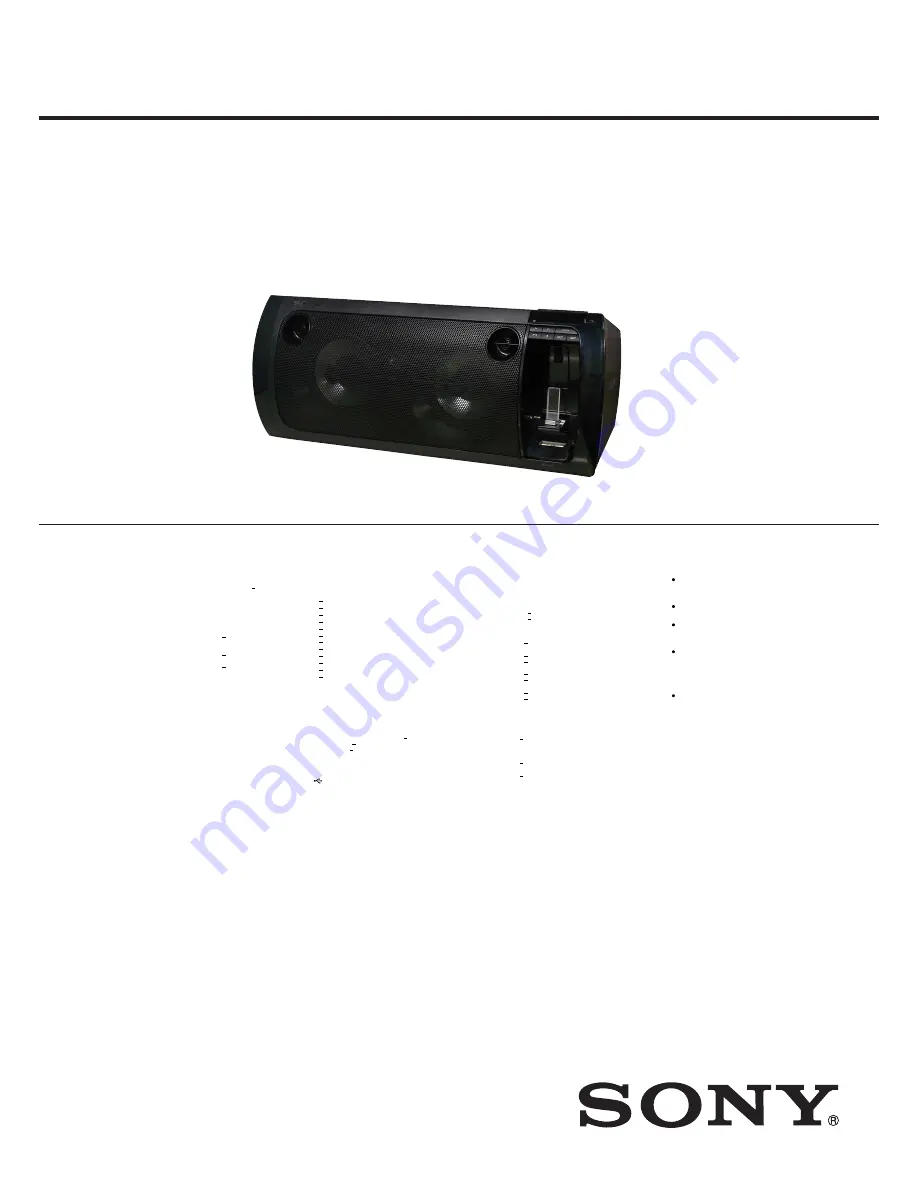
Photo: RDH-GTK33iP


