background image

35

(3)

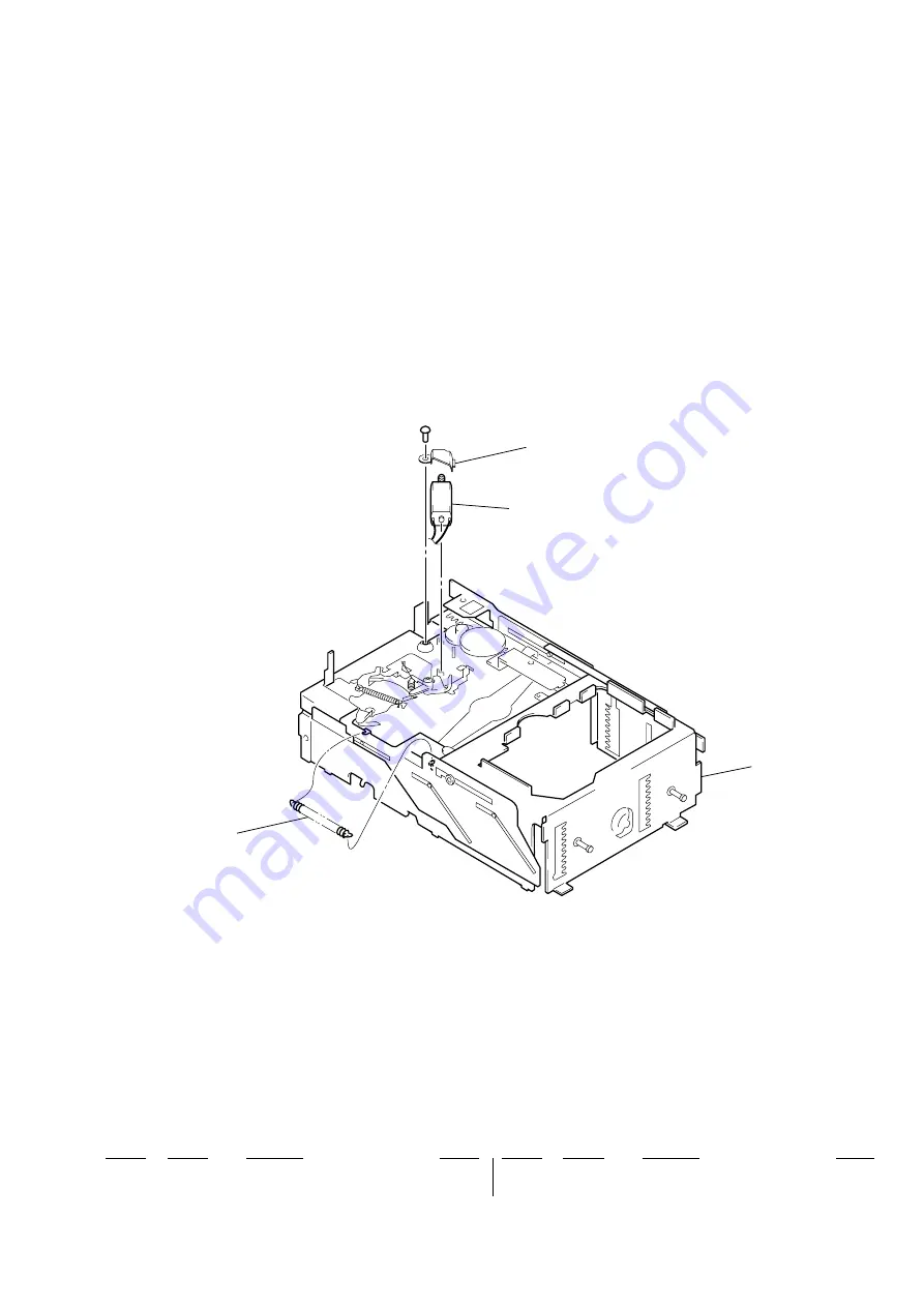
MECHANISM  DECK  SECTION-2
(MG-251A-137)

Ref. No.

Part No.

Description

Remark

Ref. No.

Part No.

Description

Remark

151

3-024-170-01 SPRING (SB), TENSION

*

152

3-040-790-01 BRACKET (EVM. S)

153

X-3378-092-1 CHASSIS (D. S) SUB ASSY

M104

A-3301-123-A ELJ MOTOR ASSY (ELEVATOR)

151

152

153

#3

M104
Summary of Contents for CDX-646 Operating Instructions (English,Español, Français)

Page 1: ... mm from the objective lens surface on the Optical Pick up Block Frequency response 10 20 000 Hz Wow and flutter Below the measurable limit Signal to noise ratio 94 dB Outputs BUS control output 8 pins Analog audio output RCA pin Current drain 800 mA during CD playback 800 mA during loading or ejecting a disc Operating temperature 10 C to 55 C 14 F to 131 F Dimensions Approx 262 90 185 mm 10 3 8 3...

Page 2: ... adjustments or performance of procedures other than those specified herein may result in hazardous ra diation exposure SERVICING NOTES NOTES ON HANDLING THE OPTICAL PICK UP BLOCK OR BASE UNIT The laser diode in the optical pick up block may suffer electro static breakdown because of the potential difference generated by the charged electrostatic load etc on clothing and the human body During repa...

Page 3: ... Installazione Installeren Vertikaal installeren Installazione in verticale Vertikaler Einbau Installation verticale Hangend installeren Als u het apparaat onder de hoedenplank of iets dergelijks wilt installeren let dan op de volgende punten Kies een geschikte plek waar u het apparaat horizontaal kunt ophangen Vergewis u ervan dat het apparaat niet beschadigd kan worden door bewegende onderdelen ...

Page 4: ...del comparto nell alloggiamento quindi inserire l angolo sinistro fino a farlo scattare in posizione Nota Non inserire il vassoio capovolto o nella direzione errata Hinweise zum Umgang mit CDs Eine verschmutzte oder beschädigte CD kann Tonaussetzer verursachen Um optimale Klangqualität sicherzustellen beachten Sie folgendes Damit die CD sauber bleibt fassen Sie sie immer am Rand an und berühren Si...

Page 5: ...ANISM DECK MG 251A 137 3 screw PTT2 6 6 4 lever FLT 838 3 screw PTT2 6 6 3 screw PTT2 6 6 1 screw PTT2 6 6 1 screw PTT2 6 6 2 front panel assy 4 lever FLT 838 5 case upper T 2 tension coil spring FL 2 tension coil spring FL 1 two dampers T filament tape 1 two dampers T 3 jack flexible board CNJ901 4 mechanism deck MG 251A 137 ...

Page 6: ... 2 jack board 2 Remove two solders of the elevator motor leads M104 2 Remove two solders of the switch board leads 2 Remove three solders of the slide variable resistor RV202 4 heat sink T 3 screw PTT2 4 6 main board 5 two screws FP 1 main flexible board CNJ101 5 screw FP 7 screw PTT2 4 8 slide variable resistor elevator height sensor RV202 ...

Page 7: ...crew PTT2 4 2 bracket EVM S 3 ELJ motor assy elevator M104 2 Remove the claw in the direction of arrow A 4 Remove the ditch in the direction of arrow B A B 5 Remove the escutcheon T in the direction of arrow C 4 ditch 3 claw C 3 two claws 1 screw T ...

Page 8: ...ree screws PTT2 4 1 screw PTT2 4 1 two screws PTT2 4 4 spring SUT 2 Remove the edge in the direction of arrow A 5 chassis U S sub assy 3 A 6 chassis assy 1 Turn the gear EVD S fully in the direction of arrow A 5 spring stopper lower 4 A 3 2 3 ...

Page 9: ...2 2 Remove two solders of the sled motor leads M101 1 OP flexible board CN102 4 RF board 1 two precision screws P2 3 4 Turn shaft feed assy in the direction of the arrow then remove it 2 sled motor assy 251 M101 OP flexible board adhesive sheet 3 optical pick up KSS 720A Q N optical pick up Note After connecting OP flexible board fix it with adhesive sheet to optical pick up ...

Page 10: ... 7 3 spring chucking 6 retainer disc 4 precision screw P2 2 2 5 bracket CP 9 Remove the spindle motor S sub assy M102 in the direction of the arrow 2 LSW board 1 precision screw P2 2 5 2 two screws PTT2 4 3 retainer CHM 4 ELJ motor assy chucking M103 1 Remove two solders of the chucking motor leads M103 ...

Page 11: ...position where the chuck plate is moved down to the lower limit A B 3 stop ring 2 0 E type 4 tension spring DH 2 optical pick up complete assy Note Insert the shaft A first shaft A gear LOAD 2 gear LOMINI marking Fig A chuck plate 2 Attach the gear LOMINI at the position shown in Fig A shaft rotary prevention C 1 Move the lever LOCK 3A fully in the direction of arrow B to move the chuck plate up B...

Page 12: ... arrow C to move down the chuck plate if the gear LOAD CAM is rotated in the direction of arrow A or the chuck plate moves up and the slider moves in the direction of arrow D if the gear is rotated in the direction of arrow B chuck plate slider gear LOAD CAM assy A B C D ...

Page 13: ... adjust the following 5 Press repeatedly the DISC and buttons on the master unit so that the elevator shafts moves from address 6 to address 5 or from 5 to 6 At this time adjust RV201 on the main board so that the elevator shaft positions smoothly between comb teeth A and B 6 Further place the set horizontally and make same adjustment as mentioned above 7 After adjustment at addresses 5 to 6 is fi...

Page 14: ...ode by loading the disc YEDS 18 3 Confirm that oscilloscope waveform is clear and check RF sig nal level is correct or not Note Clear RF signal waveform means that the shape can be clearly distin guished at the center of the waveform When observing the eye pattern set the oscilloscope to AC range and raise the vertical sensitivity so that it may be easily seen GND BUS cable compact disc changer ma...

Page 15: ...on the master unit and check the traverse waveform 4 Confirm that the oscilloscope waveform is symmetrical on the top and bottom in relation to 0 V dc and check this level Traverse waveform This is the tracking error wave form appears when crossing the track oscilloscope DC range TP VC TP TE IC101 A B 0 V A B traverse waveform 100 track jump waveform VOLT DIV 500 mV TIME DIV 2 ms Center 0 V Traver...

Page 16: ...16 MEMO ...

Page 17: ...A D CONVERTER MIRR DFCT FOK DIGITAL SERVO SIGNAL PROCESS PWM GENERATOR 40 41 25 24 TEDR TRDR VIN1 B 18 8 9 VO3 VO3 VIN3 VIN3 DIGITAL CLV 35 MDP M M103 CHUCKING M102 SPINDLE M101 SLED TRACKING FOCUS COIL DRIVE SLED SPINDLE CHUCKING MOTOR DRIVE IC201 MOTOR DRIVE COIL DRIVE SERVO AUTO SEQUENCER SERVO INTERFACE 94 CH F 71 CH R 72 89 11 XRST 36 SSTP LIMSW SW3 LIMIT 65 LOAD1 SW2 SAVE END DETECT 66 LOAD2...

Page 18: ...ERFACE FOR SONY BUS IC302 5V REGULATOR IC305 5V REGULATOR IC303 DAC SERVO 5V Z SW801 76 MGLK 74 ELVF 73 ELVR SW201 MAGAZINE DETECT ON When magazine is set 3 4 40 XTAL 41 EXTAL 9 7 MOTOR DRIVE IN1 IN2 OUT1 OUT2 ELEVATOR MOTOR DRIVE IC301 M M104 ELEVATOR X201 12MHz B UP 5V SYSTEM CONTROLLER IC201 2 2 05 RESET 10 6 9 11 4 1 12 13 2 8 7 SO SI SCK BUSON OUT BUSON OUT RESET DATA 14 CLK LOF BUSON IN RST ...

Page 19: ...ation U B Line H adjustment for repair Power voltage is dc 14 4V and fed with regulated dc power supply from CD changer controller Voltages and waveforms are dc with respect to ground under no signal conditions no mark CD PLAY Impossible to measure Voltages are taken with aVOM Input impedance 10 MΩ Voltage variations may be noted due to normal produc tion tolerances Waveforms are taken with a osci...

Page 20: ...20 20 CDX 646 646X 6 4 PRINTED WIRING BOARDS LSW RF Boards See page 19 for Circuit Boards Location Semiconductor Location RF Board Component Side Ref No Location IC101 H 4 IC201 I 3 Q101 F 4 Page 22 ...

Page 21: ...28 for IC Block Diagrams The components identified by mark 0 or dotted line with mark 0 are critical for safety Replace only with part number specified Les composants identifiés par une marque 0 sont critiques pour la sécurité Ne les remplacer que par une pièce portant le numéro spécifié Page 24 ...

Page 22: ...r Circuit Boards Location Semiconductor Location Ref No Location D302 D 2 D303 D 3 D306 F 4 D307 F 4 D309 F 4 D310 F 3 D313 D 3 D314 C 3 D315 C 3 IC101 C 8 IC201 E 8 IC301 G 3 IC302 D 3 IC303 F 3 IC401 C 6 Q201 E 10 Q301 F 5 Q302 F 5 Q303 F 4 Q403 E 5 Q410 D 5 Q420 D 5 Page 26 Page 20 ...

Page 23: ...23 23 CDX 646 646X 6 7 PRINTED WIRING BOARD MAIN Board Conductor Side See page 19 for Circuit Boards Location Semiconductor Location Ref No Location IC304 G 1 IC305 E 1 Page 26 ...

Page 24: ...24 24 CDX 646 646X 6 8 SCHEMATIC DIAGRAM MAIN Board 1 2 See page 27 for Waveforms See page 28 for IC Block Diagram Page 21 ...

Page 25: ...25 25 CDX 646 646X 6 9 SCHEMATIC DIAGRAM MAIN Board 2 2 See page 27 for Waveform See page 28 for IC Block Diagrams Page 26 Page 26 ...

Page 26: ...26 26 CDX 646 646X 6 10 PRINTED WIRING BOARDS JACK SWITCH Boards See page 19 for Circuit Boards Location 6 11 SCHEMATIC DIAGRAM JACK SWITCH Boards Page 22 Page 23 Page 25 Page 25 ...

Page 27: ...3 IC101 qd TE CD play mode 2 IC101 ia BCK is BCKI CD play mode 3 IC101 ih XTAI CD play mode 4 IC201 ra EXTAL CD play mode 1 4 0 3 Vp p Apporx 63 mVp p Approx 63 mVp p MAIN Board 1 IC101 uj LRCK uk LRCKI CD play mode 5 7 Vp p 470 ns 5 6 Vp p 22 8 µs 4 1 Vp p 60 ns 4 4 Vp p 83 ns ...

Page 28: ...PUT FWD REV VCC2 VLO VLO VO4 VO4 VO3 VO3 VO2 VO2 VO1 VO1 VCC1 VIN1 VIN1 A VIN1 A VIN1 B S GND MUTE2 MUTE1 VIN4 VIN4 VIN4 VREF IN VIN1 VREF SW VREF OUT CH1 REG OUT REG IN VIN3 VIN3 VIN3 VIN2 VIN2 VIN2 VIN1 B OUTPUT CONTROL LEVEL SHIFT CH2 4 MUTE THERMAL SHUT DOWN CH1 MUTE VIN1 VREF SWITCH 5VREG 3 4 5 6 7 8 9 2 1 LEVEL SHIFT LEVEL SHIFT 10 11 14 LEVEL SHIFT AMP A AMP B 15 16 17 18 23 19 34 35 36 25 ...

Page 29: ...G SERVO SLED SERVO INTERNAL BUS PWM 100 LOW PASS FILTER PWM BCK BCKI ENPH EMPHI XVDD XTAI XTAO XVSS AVDD1 AOUT1 AIN1 LOUT1 AVSS1 AVSS2 LOUT2 AIN2 RMUT AOUT2 AVDD2 LMUT PCMDI PCMD LRCKI LRCK VDD ASYE DOUT MD2 VSS VPCO V16M VCTL BIAS AVDD3 PCO FILI FILO CLTV AVSS3 RFAC ASYI ASYO AVDD0 IGEN AVSS0 ADIO RFDC CE TE SE FE VC TES1 XTSL VSS VDD FRDR FFDR TRDR TFDR SRDR SFDR TEST FSTIO SSTP MDP LOCK PWMI FO...

Page 30: ...T I System reset signal input from the SONY bus interface IC302 and reset signal generator IC303 L reset For several hundreds msec after the power supply rises L is input then it changes to H 39 GND Ground terminal 40 XTAL O Main system clock output terminal 12 MHz 41 EXTAL I Main system clock input terminal 12 MHz 42 TEXTSEL I CD text mode setting terminal L CD text on H does not display track na...

Page 31: ... 76 MGLK I Magazine detect switch SW201 input L magazine is set 77 SQSO O Subcode Q text serial data output to the CXD2598Q IC101 78 NC Not used open 79 SQCK O Subcode Q text serial data transfer clock signal output to the CXD2598Q IC101 80 GRSCOR I Subcode sync S0 S1 detection signal input terminal Not used open 81 NC Not used open 82 SCOR I Subcode sync S0 S1 detection signal input from the CXD2...

Page 32: ...r M104 control STOP ELEVATOR UP ELEVATOR DOWN BRAKE ELVF pin uf H L H L ELVR pin ud H H L L Mode Terminal 1 chucking motor M103 control STOP LOAD CHUCKING SAVE BRAKE CH F pin ua H H L L CH R pin us H L H L Mode Terminal ...

Page 33: ...ts Color Cabinet s Color Ref No Part No Description Remark Ref No Part No Description Remark 1 3 047 852 01 DAMPER T 2 3 045 543 01 CASE LOWER T 3 3 024 065 01 CUSHION EJECT T 4 X 3375 357 1 ARM FLT ASSY 5 1 675 515 11 JACK BOARD 6 3 376 464 11 SCREW PTT 2 6X6 GROUND POINT 7 A 3294 822 A MAIN BOARD COMPLETE 8 1 676 340 11 JACK FLEXIBLE BOARD 9 1 676 339 11 MAIN FLEXIBLE BOARD 10 1 675 516 11 SWITC...

Page 34: ...DECK SECTION 1 MG 251A 137 Ref No Part No Description Remark Ref No Part No Description Remark 101 X 3378 091 1 CHASSIS U S SUB ASSY 102 3 024 161 11 SPRING SUT 103 3 011 997 01 SPRING STOPPER LOWER 3 3 3 101 102 103 ...

Page 35: ...A 137 Ref No Part No Description Remark Ref No Part No Description Remark 151 3 024 170 01 SPRING SB TENSION 152 3 040 790 01 BRACKET EVM S 153 X 3378 092 1 CHASSIS D S SUB ASSY M104 A 3301 123 A ELJ MOTOR ASSY ELEVATOR 151 152 153 3 M104 ...

Page 36: ...CKET CHM D ASSY 204 3 321 813 01 WASHER COTTER POLYETHYLENE 205 3 017 139 01 GEAR WORM LOAD A 206 3 022 839 01 ARM NSW 207 3 573 936 00 STOPPER REEL 208 X 3375 220 1 GEAR LOAD CAM ASSY 209 3 010 252 11 ROLLER CRE 210 3 010 268 01 SPRING DH TENSION 211 A 3290 194 C MAIN ASSY CHASSIS EVY 212 3 010 254 11 SHAFT ROTARY PREVENTION C 213 3 010 253 01 GEAR LOMINI 214 A 3326 000 A RF BOARD COMPLETE M103 A...

Page 37: ...emark Ref No Part No Description Remark 251 1 676 341 11 OP FLEXIBLE BOARD 252 3 025 743 01 SPRING FEED LEAF 253 X 3378 101 1 HOLDER SLED S ASSY 254 3 931 832 01 GEAR SL MIDWAY 0255 8 820 103 05 OPTICAL PICK UP KSS 720A Q RP 256 A 3291 669 A SHAFT FEED ASSY 257 3 010 263 01 DETENT SHAFT THRUST 258 1 676 524 11 LSW BOARD 259 A 3301 954 A BASE OPT S J ASSY M101 A 3315 151 A SLED MOTOR ASSY 251 M102 ...

Page 38: ... 1 126 382 11 ELECT 100uF 20 16V C145 1 126 382 11 ELECT 100uF 20 16V C201 1 107 826 11 CERAMIC CHIP 0 1uF 10 16V C203 1 164 360 11 CERAMIC CHIP 0 1uF 16V C204 1 164 360 11 CERAMIC CHIP 0 1uF 16V C205 1 164 360 11 CERAMIC CHIP 0 1uF 16V C301 1 164 360 11 CERAMIC CHIP 0 1uF 16V C302 1 164 360 11 CERAMIC CHIP 0 1uF 16V C303 1 164 360 11 CERAMIC CHIP 0 1uF 16V C304 1 164 360 11 CERAMIC CHIP 0 1uF 16V...

Page 39: ... 2 1 16W R141 1 218 871 11 RES CHIP 10K 2 1 16W R142 1 218 871 11 RES CHIP 10K 2 1 16W R143 1 218 871 11 RES CHIP 10K 2 1 16W R144 1 218 871 11 RES CHIP 10K 2 1 16W R145 1 218 871 11 RES CHIP 10K 2 1 16W R201 1 216 821 11 METAL CHIP 1K 5 1 16W R207 1 216 845 11 METAL CHIP 100K 5 1 16W R209 1 216 833 11 METAL CHIP 10K 5 1 16W R301 1 216 841 11 METAL CHIP 47K 5 1 16W R302 1 216 845 11 METAL CHIP 100...

Page 40: ...3 1 216 833 11 METAL CHIP 10K 5 1 16W R214 1 216 839 11 METAL CHIP 33K 5 1 16W R215 1 216 839 11 METAL CHIP 33K 5 1 16W R216 1 216 842 11 METAL CHIP 56K 5 1 16W R218 1 216 839 11 METAL CHIP 33K 5 1 16W R219 1 216 843 11 METAL CHIP 68K 5 1 16W R220 1 216 834 11 METAL CHIP 12K 5 1 16W R222 1 216 821 11 METAL CHIP 1K 5 1 16W R223 1 216 821 11 METAL CHIP 1K 5 1 16W SWITCH SW1 1 529 566 21 SWITCH PUSH ...

Page 41: ...STALLATION AND CONNECTIONS 501 3 040 583 21 BRACKET T 502 X 3369 824 1 SCREW ASSY 503 1 590 874 11 CORD CONNECTION RCA PIN CORD 5 5m 504 1 590 519 21 CORD WITH CONNECTOR BUS CABLE 5 5m 501 502 PSW4 10 4 TAPPING SCREW DIA 5 20 4 BRACKET 2 503 504 RCA PIN CORD 5 5 m 1 BUS CABLE 5 5 m 1 ...

Page 42: ...42 CDX 646 646X Sony Corporation Audio Entertainment Group 9 870 218 11 2000L0562 1 Printed in Japan C 2000 12 Published by General Engineering Dept ...

Reviews: