


26
CDP-M400CS
Electrical Adjustment
Note:
1. CD Block is basically designed to operate without adjustment.
Therefore, check each item in order given.
2. Use YEDS-18 disc (3-702-101-01) unless otherwise indicated.
3. Use an oscilloscope with more than 10M
Ω
impedance.
4. Clean the object lens by an applicator with neutral detergent
when the signal level is low than specified value with the
following checks.
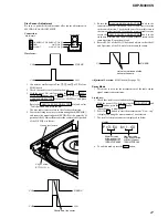
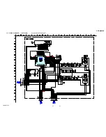
S-Curve Check
Procedure :
1. Chuck the disc (YEDS-18) beforehand.
2. Connect oscilloscope to test point TP (FE1) on BD board.
3. With the power ON, while pressing the TIME and MEGA
CONTROL buttons, press the
1/u
button.
Rotate the DISC/ALBUM/CHARACTER dial, select “BU
Test” and press the dial.
4. Rotate the DISC/ALBUM/CHARACTER dial, and select
“bdt S CURVE”. Press the dial “LD AL” is displayed.
5. Check the oscilloscope waveform (S-curve) is symmetrical
between A and B. And confirm peak to peak level within 3
±
1
Vp-p.
S-curve waveform
6. Pressing the MENU/NO button stops the output of the
waveform (S CURVE). “bdt S CURVE”is displayed.
7. To end this mode, press the
?/1
button.
Note : • Try to measure several times to make sure than the ratio
of A : B or B : A is more than 10 : 7.
• Take sweep time as long as possible and light up the
brightness to obtain best waveform.
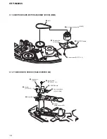
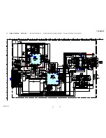
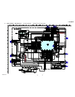
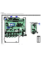
Adjustment Location: BD board (See page 28)
RF Level Check
oscilloscope
BD board
TP (FE1)
TP (DVC)
symmetry
A
B
Within 3
±
1 Vp-p
VOLT/DIV : 1V
TIME/DIV : 400
µ
s
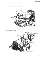
oscilloscope
BD board
TP (RFAC)
TP (DVC)
VOLT/DIV : 500mV
TIME/DIV : 1
µ
s
level : 1.2 Vp-p
+0.25
–0.20
Procedure :
1. Connect oscilloscope to test point TP (RFAC) on BD board.
2. Turn Power switch on.
3. Put disc (YEDS-18) in to play the number five track.
4. Confirm that oscilloscope waveform is clear and check RF
signal level is correct or not.
Note : A clear RF signal waveform means that the shape “
◊
”
can be clearly distinguished at the center of the waveform.
RF signal waveform
Adjustment Location: BD board (See page 28)
Summary of Contents for CDP-M400CS Operating Instructions (CDPM400CS)
Page 69: ...69 CDP M400CS MEMO ...