


Rev 3.0 Aug.19
26
41111116
B
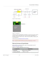
Appendix B: 50 Ω Antenna Matching
We used the
AppCAD
tool to simulate 50
Ω
impedance for the RF PCB layout.
Figure B-1: Dimensions
Notice
:
For multi-layer layouts, you can place a ground layer in the second layer to minimize
the trace width in a specific PCB (such as FR4) and impedance.
For impedance calculation, there is free software available to calculate the trace width
or impedance. Once such software package is:
http://www.awrcorp.com/products/additional-products/tx-line-transmission-line-
calculator
Table B-1: Antenna Matching
RF Line Width (W)
PCB FR4
Thickness
Dielectric
Parameters
Copper Thickness
per ounce
1.8mm
1mm
4.6
0.035mm