background image

Communication 


8.6 RS485 


S7-200 SMART 

462


System Manual, V2.3, 07/2017, A5E03822230-AF 

8.6.5.6


Biasing and terminating the network cable 

Siemens provides two types of network connectors that you can use to easily connect 

multiple devices to a network:  


Standard network connector 


Connector that includes a port which allows you to connect an HMI device to the network 

without disturbing any existing network connections 

The programming port connector passes all signals (including the power pins) from the 

S7-200 SMART CPU through to the programming port, which is especially useful for 

connecting devices that draw power from the S7-200 SMART CPU (such as a TD 400C).  
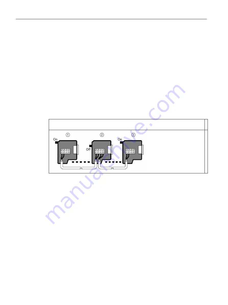
Both connectors have two sets of terminal screws to allow you to attach the incoming and 

outgoing network cables. Both connectors also have switches to bias and terminate the 

network selectively. The following shows typical biasing and termination for the cable 

connectors.  

Table 8- 19  Biasing and termination for cable connectors 

Cable must be terminated and biased at both ends. Bare shielding: Approximately 12 mm (1/2 in) 

must contact the metal guides of all locations. 


 Switch position = On: Terminated and biased 

 Switch position = Off: No termination or bias 

 Switch position = On: Terminated and biased 


Summary of Contents for SIMATIC S7-200

Page 1: ...____________ ___________________ ___________________ SIMATIC S7 S7 200 SMART System Manual V2 3 07 2017 A5E03822230 AF Preface Product overview 1 Getting started 2 Installation 3 PLC concepts 4 Programming concepts 5 PLC device configuration 6 Program instructions 7 Communication 8 Libraries 9 Debugging and troubleshooting 10 PID loops and tuning 11 Open loop motion control 12 Technical specificat...

Page 2: ...ly by personnel qualified for the specific task in accordance with the relevant documentation in particular its warning notices and safety instructions Qualified personnel are those who based on their training and experience are capable of identifying risks and avoiding potential hazards when working with these products systems Proper use of Siemens products Note the following WARNING Siemens prod...

Page 3: ...of automation and programmable logic controllers Scope of the manual This manual describes the following products STEP 7 Micro WIN SMART V2 3 S7 200 SMART CPU firmware release V2 3 For a complete list of the S7 200 SMART products and article numbers described in this manual see Technical Specifications Page 679 Certification CE label and other standards Refer to the technical specifications for mo...

Page 4: ...cted to the enterprise network or the internet if and to the extent necessary and with appropriate security measures e g use of firewalls and network segmentation in place Additionally Siemens guidance on appropriate security measures should be taken into account For more information about industrial security please visit http www siemens com industrialsecurity Siemens products and solutions under...

Page 5: ...communication with the CPU 37 2 2 Creating the sample program 39 2 2 1 Network 1 Starting the timer 40 2 2 2 Network 2 Turning the output on 41 2 2 3 Network 3 Resetting the timer 42 2 2 4 Setting the CPU type and version for your project 43 2 2 5 Saving the sample project 44 2 3 Downloading the sample program 45 2 4 Changing the operating mode of the CPU 46 3 Installation 47 3 1 Guidelines for in...

Page 6: ...erting a memory card in a standard CPU 96 4 3 6 Transferring your program with a memory card 97 4 3 7 Restoring data after power on 99 4 4 Changing the operating mode of the CPU 100 4 5 Status LEDs 101 5 Programming concepts 103 5 1 Guidelines for designing a PLC system 103 5 2 Elements of the user program 105 5 3 Creating your user program 108 5 3 1 Earlier versions of STEP 7 Micro WIN projects 1...

Page 7: ...a reset to factory defaults memory card 167 6 2 High speed I O 168 7 Program instructions 169 7 1 Bit logic 169 7 1 1 Standard inputs 169 7 1 2 Immediate inputs 171 7 1 3 Logic stack overview 172 7 1 4 STL logic stack instructions 174 7 1 5 NOT 176 7 1 6 Positive and negative transition detectors 177 7 1 7 Coils output and output immediate instructions 178 7 1 8 Set reset set immediate and reset i...

Page 8: ...act multiply and divide 297 7 8 2 Multiply integer to double integer and divide integer with remainder 300 7 8 3 Trigonometry natural logarithm exponential and square root 302 7 8 4 Increment and decrement 305 7 9 PID 307 7 9 1 Using the PID wizard 308 7 9 2 PID algorithm 313 7 9 3 Converting and normalizing the loop inputs 317 7 9 4 Converting the loop output to a scaled integer value 318 7 9 5 F...

Page 9: ...tion ports 397 8 3 HMIs and communication drivers 398 8 4 Ethernet 400 8 4 1 Overview 400 8 4 2 Local partner connection 400 8 4 3 Sample Ethernet network configurations 401 8 4 4 Assigning Internet Protocol IP addresses 402 8 4 4 1 Assigning IP addresses to programming and network devices 402 8 4 4 2 Configuring or changing an IP address for a CPU or device in your project 404 8 4 4 3 Searching f...

Page 10: ...tances transmission rates and cable lengths for your network 459 8 6 5 3 Repeaters on the network 459 8 6 5 4 Specifications for RS485 cable 460 8 6 5 5 Connector pin assignments 460 8 6 5 6 Biasing and terminating the network cable 462 8 6 5 7 Biasing and terminating the CM01 signal board 463 8 6 5 8 Using HMI devices on your RS485 network 464 8 6 6 Freeport mode 465 8 6 6 1 Creating user defined...

Page 11: ...table 536 9 4 4 4 Passive partner server 537 9 4 4 5 CheckErrors subroutine 543 9 4 4 6 Passive partner symbol table 544 9 5 USS library 545 9 5 1 USS communication overview 545 9 5 1 1 USS protocol overview 545 9 5 1 2 Requirements for using the USS protocol 546 9 5 1 3 Calculating the time required for communicating with the drive 547 9 5 2 USS program instructions 548 9 5 2 1 Using the USS prot...

Page 12: ...04 12 4 Programming an Axis of Motion 606 12 5 Configuring an Axis of Motion 607 12 6 Subroutines created by the Motion wizard for the Axis of Motion 620 12 6 1 Guidelines for using the Motion subroutines 621 12 6 2 AXISx_CTRL subroutine 622 12 6 3 AXISx_MAN subroutine 623 12 6 4 AXISx_GOTO subroutine 625 12 6 5 AXISx_RUN subroutine 626 12 6 6 AXISx_RSEEK subroutine 627 12 6 7 AXISx_LDOFF subrouti...

Page 13: ... specifications 679 A 2 S7 200 SMART CPUs 685 A 2 1 CPU ST20 CPU SR20 and CPU CR20s 685 A 2 1 1 General specifications and features 685 A 2 1 2 Digital inputs and outputs 689 A 2 1 3 Wiring diagrams 692 A 2 2 CPU ST30 CPU SR30 and CPU CR30s 695 A 2 2 1 General specifications and features 695 A 2 2 2 Digital inputs and outputs 698 A 2 2 3 Wiring diagrams 701 A 2 3 CPU ST40 CPU SR40 and CPU CR40s 70...

Page 14: ...1 A 8 1 SB RS485 RS232 specifications 771 A 9 Battery board signal boards SBs 773 A 9 1 SB BA01 Battery board 773 A 10 EM DP01 PROFIBUS DP module 775 A 10 1 S7 200 SMART CPUs that support the EM DP01 PROFIBUS DP module 776 A 10 2 Connector pin assignments for EM DP01 777 A 10 3 EM DP01 PROFIBUS DP module wiring diagram 778 A 11 S7 200 SMART cables 779 A 11 1 S7 200 SMART I O expansion cable 779 A ...

Page 15: ...45 HSC3 SMB146 SMB155 HSC4 SMB156 SMB165 HSC5 high speed counters 810 D 15 SMB66 SMB85 PTO0 PWM0 PTO1 PWM1 SMB166 SMB169 PTO0 SMB176 SMB179 PTO1 and SMB566 SMB579 PTO2 PWM2 high speed outputs 816 D 16 SMB86 SMB94 and SMB186 SMB194 Receive message control 819 D 17 SMW98 Expansion I O bus communication errors 821 D 18 SMW100 SMW114 System alarms 822 D 19 SMB130 Freeport control for port 1 See SMB30 ...

Page 16: ...in priority order 832 E 3 High speed counter summary 833 E 4 STL instructions 834 E 5 Memory ranges and features 841 F Ordering information 843 F 1 CPU modules 843 F 2 Expansion modules EMs and signal boards SBs 844 F 3 Programming software 844 F 4 Communication 845 F 5 Spare parts and other hardware 845 F 6 Human Machine Interface devices 847 Index 849 ...

Page 17: ...pport your automation needs The CPU monitors inputs and changes outputs as controlled by the user program which can include Boolean logic counting timing complex math operations and communications with other intelligent devices The compact design flexible configuration and powerful instruction set combine to make the S7 200 SMART a perfect solution for controlling a wide variety of applications ...

Page 18: ...t communication port Clip for installation on a standard DIN rail Ethernet status LEDs under door LINK Rx Tx Status LEDs RUN STOP and ERROR RS485 Communication port Optional signal board Standard models only Memory card reader under door Standard models only The CPU provides different models with a diversity of features and capabilities that help you create effective solutions for your varied appl...

Page 19: ... User memory Program 12 Kbytes 12 Kbytes 12 Kbytes 12 Kbytes User data 8 Kbytes 8 Kbytes 8 Kbytes 8 Kbytes Retentive 2 Kbytes max 1 2 Kbytes max 1 2 Kbytes max 1 2 Kbytes max 1 On board digi tal I O Inputs Outputs 12 DI 8 DQ Relay 18 DI 12 DQ Relay 24 DI 16 DQ Relay 36 DI 24 DQ Relay Expansion modules None None None None Signal board None None None None High speed counters 4 total Single phase 4 a...

Page 20: ...z 5 at 200 kHz 1 at 30 kHz 4 at 200 kHz 2 at 30 kHz 4 at 200 kHz 2 at 30 kHz A B phase 2 at 100 kHz 2 at 20 kHz 3 at 100 kHz 1 at 20 kHz 2 at 100 kHz 2 at 20 kHz 2 at 100 kHz 2 at 20 kHz Pulse outputs 2 2 at 100 kHz 3 at 100 kHz 3 at 100 kHz 3 at 100 kHz PID loops 8 8 8 8 Real time clock with 7 day back up Yes Yes Yes Yes 1 You can configure areas of V memory M memory C memory current values and p...

Page 21: ...does not apply to the CPU CR40 and CPU CR60 models Status LED states All CPU models now blink the STOP LED at 1 Hz if a value is forced in RUN or STOP mode High Speed Counters HSC New HSC capabilities are as follows The number of HSCs increased from four to six on the SR and ST CPU models The new CRs CPUs have four HSCs The SR ST30 CPUs now utilize the high speed inputs I0 6 and I0 7 for HSC4 This...

Page 22: ...rt Signal board port DP01 PROFIBUS port See also Creating a user defined library of instructions Page 563 EM DE08 and EM DE16 digital input specifications Page 725 EM DT08 EM DR08 EM QR16 and EM QT16 digital output specifications Page 727 S7 200 SMART I O expansion cable Page 779 Using STEP 7 Micro WIN SMART to create your programs Page 111 Modbus RTU library Page 476 Open user communication libra...

Page 23: ...d CPU CR60s models have the following differences from the standard CPUs No Ethernet port The RS485 port is now the programming port STEP 7 Micro WIN SMART uses a USB PPI cable to program the CPU through the RS485 port The CPUs reserve one connection for the STEP 7 Micro WIN SMART programmer connection No CPU instructions that require an Ethernet port No support for data logs No real time clock No...

Page 24: ...thernet port You cannot use the CPU instructions that utilize the Ethernet port on the CRs models The instructions that are not available in the CRs models are as follows LAD instruction STL instruction Description GET GET Get data through the Ethernet SET SET Write data through the Ethernet GIP_ADDR GIP Get Ethernet IP address SIP_ADDR SIP Set Ethernet IP address TCON TCON Open an OUC Ethernet co...

Page 25: ...g PROFIBUS RS485 capable HMIs COMFORT HMIs SIMATIC HMI TP700 COMFORT SIMATIC HMI TP900 COMFORT SIMATIC HMI TP1200 COMFORT SIMATIC HMI KP400 COMFORT SIMATIC HMI KP700 COMFORT SIMATIC HMI KP900 COMFORT SIMATIC HMI KP1200 COMFORT SIMATIC HMI KTP400 COMFORT SMART HMIs SMART 700 IE SMART 1000 IE BASIC HMIs SIMATIC HMI KTP600 BASIC COLOR DP SIMATIC HMI KTP1000 BASIC COLOR DP Micro HMIs TD 400C TEXT DISP...

Page 26: ... about a specific module see the technical specifications Page 679 Table 1 4 Expansion modules and signal boards Type Input only Output only Combination In Out Other Digital expan sion module 8 x DC In 16 x DC In 8 x DC Out 8 x Relay Out 16 x Relay Out 16 x DC Out 8 x DC In 8 x DC Out 8 x DC In 8 x Relay Out 16 x DC In 16 x DC Out 16 x DC In 16 x Relay Out Analog expan sion modules 4 x Analog In 8...

Page 27: ...tion The TD400C device provides a low cost interface to your application by allowing you to view monitor and change the process variables pertaining to your application SMART HMIs The SMART LINE Touch Panel provides operating and monitoring functions for small scale machines and plants Short configura tion and commissioning times their configuration in WinCC flexible ASIA version and a double port...

Page 28: ...hernet communications PROFIBUS High speed communications for distributed I O up to 12 Mbps One bus master connects to many I O devices supports 126 addressable devices Exchange of data between the master and I O devices EM DP01 module is a PROFIBUS I O device RS485 Provides a STEP 7 Micro WIN SMART connection for programming when using a USB PPI cable Supports a total of 126 addressable devices 32...

Page 29: ...To help you find the information you need STEP7 Micro WIN SMART provides an extensive online help system Computer requirements STEP 7 Micro WIN SMART runs on a personal computer Your computer should meet the following minimum requirements Operating system Windows 7 or Windows 10 both 32 bit and 64 bit versions At least 350M bytes of free hard disk space Mouse recommended Installing STEP 7 Micro WI...

Page 30: ...Product overview 1 7 Programming software S7 200 SMART 30 System Manual V2 3 07 2017 A5E03822230 AF ...

Page 31: ...Note The CPU models CPU CR20s CPU CR30s CPU CR40s and CPU CR60s have no Ethernet port and no functions related to the use of Ethernet communications Connecting power to the CPU WARNING Ensure power is off prior to installing wiring or removing devices Before you install or remove any electrical device ensure that the power to that equipment has been turned off Attempts to install or connect the wi...

Page 32: ...C model of the CPU DC installation AC installation 2 1 1 Configuring the CPU for communication 2 1 1 1 Overview A CPU can communicate with a STEP 7 Micro WIN SMART programming device on two types of communications networks A CPU can communicate with a STEP 7 Micro WIN SMART programming de vice on an Ethernet network A CPU can communicate with a STEP 7 Micro WIN SMART programming de vice on an RS48...

Page 33: ... do not support any functions related to the use of Ethernet communications 2 1 1 2 Establishing the Ethernet hardware communication connection The Ethernet interfaces establish the physical connections between a programming device and a CPU Since Auto Cross Over functionality is built into the CPU either a standard or crossover Ethernet cable can be used for the interface An Ethernet switch is no...

Page 34: ...he navigation bar Select Communications from the Component drop down list in the Windows area of the View menu ribbon strip The Communications dialog provides two methods of selecting the CPU to be accessed Click the Find CPUs button to have STEP 7 Micro WIN SMART search your local network for CPUs The IP address of each CPU found on the network is listed under Found CPUs Click the Add CPU button ...

Page 35: ...r your Communication Inter face Click the Add CPU button to do one of the following Enter the IP address of a CPU that is ac cessible from the programming device but is not on the local network Enter the IP address of a CPU directly that is on the local network All CPUs have a default IP address See the Note below Highlight a CPU and then click OK After you have established communication with the ...

Page 36: ...you can change the IP address of the CPU to match the network class and subnet of your network interface card See the Configuring or changing an IP address for a CPU or device in your project for information about how to accomplish this 2 1 1 4 Establishing the RS485 hardware communication connection The RS485 interfaces establish the physical connections between a programming device and a CPU Fol...

Page 37: ...ud rate After you have established communication with the CPU you are ready to create and download the example program To download all project components click the Download button from the Transfer area of the File or PLC menu ribbon strip or alternatively press the shortcut key combination CTRL D If STEP 7 Micro WIN SMART does not find your CPU check the settings for the communications parameters...

Page 38: ...CPUs button to display all operational CPUs Found CPUs on the RS485 network All CPUs default their RS485 network settings to address 2 and 9 6 Kbps Highlight a CPU and then click OK Note You can open multiple copies of STEP 7 Micro WIN SMART on a computer Be aware that when you open a second copy of STEP 7 Micro WIN SMART or use the Find CPUs button in either copy the communication connection to t...

Page 39: ...ription column explains the logic for each network The timing diagram shows the operation of the program There are no network comments in the STL program Table 2 1 Sample program for getting started with STEP 7 Micro WIN SMART LAD FBD STL Description Network 1 LDN M0 0 TON T33 100 10 ms timer T33 times out after 100 x 10 ms 1 s M0 0 pulse is too fast to monitor with Status view Network 2 LDW T33 4...

Page 40: ... toolbar icons pro vide shortcuts to PLC commands and programming operation After you enter and save the program you can download the program to the CPU 2 2 1 Network 1 Starting the timer Network 1 Starting the timer When M0 0 is off 0 this contact turns on and provides power flow to start the timer To enter the contact for M0 0 1 Either double click the Bit Logic icon or click the plus sign to di...

Page 41: ...Network 2 Turning the output on Network 2 Turning the output on When the timer value for T33 is great er than or equal to 40 40 times 10 milliseconds or 0 4 seconds the contact provides power flow to turn on output M10 0 of the CPU To enter the Compare instruction 1 Double click the Compare icon to display the compare instructions Select the I instruction greater than or equal to integer 2 Hold do...

Page 42: ...rns on Power flow from this contact turns on the M0 0 memory location Because the timer is enabled by a Normally Closed contact for M0 0 changing the state of M0 0 from off 0 to on 1 resets the timer To enter the contact for the timer bit of T33 1 Select the Normally Open contact from the bit logic instructions 2 Hold down the left mouse button and drag the contact onto the third network 3 Click a...

Page 43: ...or the CPU and version matching your physical CPU If the project is not configured for the correct CPU and CPU version then the download could fail or the program may not run To select your CPU click the CPU field under the Module column to display the dropdown list button and select your CPU from the dropdown list Using the same procedure select your CPU version in the Version column ...

Page 44: ...s the CPU type and other parameters To save the project in a file name and location that you specify 1 Click the down arrow under the Save button from the Operations area of the File menu ribbon strip to display the Save As button 2 Click the Save As button and provide a filename for saving your project 3 Enter a name for the project in the Save As dialog 4 Browse to a location where you want to s...

Page 45: ...ribbon strip or alternatively press the shortcut key combination CTRL D Click the Download dialog Down load button STEP 7 Micro WIN SMART cop ies the complete program or pro gram components that you selected to the CPU If your CPU is in RUN mode a dialog prompts you to place the CPU in STOP mode Clicking Yes sets the CPU to STOP mode Note Each project is associated with a CPU type If the project t...

Page 46: ...ownload program blocks Placing the CPU in RUN mode 1 Click the RUN button on either the PLC menu ribbon strip or on the program editor toolbar 2 When prompted click OK to change the operating mode of the CPU You can monitor the program in STEP 7 Micro WIN SMART by clicking the Program Status button from the Debug menu ribbon strip or from the program editor toolbar STEP 7 Micro WIN SMART displays ...

Page 47: ...requirements could result in death or serious injury to personnel and or damage to equipment Always follow these requirements when installing the PLC Separate the devices from heat high voltage and electrical noise As a general rule for laying out the devices of your system always separate the devices that generate high voltage and high electrical noise from the low voltage logic type devices such...

Page 48: ...losure CAUTION Temperature considerations Vertical mounting reduces the maximum allowable ambient temperature by 10 degrees C Operating outside the maximum temperature range could result in erratic process operation and could result in minor personal injury If your installation includes expansion modules mount the CPU below them as shown in the following figure Follow the prescribed guidelines for...

Page 49: ... may not be able to connect the maximum number of modules allowed for your CPU The standard CPU also provides a 24 V DC sensor supply that can supply 24 V DC for input points for relay coil power on the expansion modules or for other requirements If your power requirements exceed the budget of the sensor supply then you must add an external 24 V DC power supply to your system You must manually con...

Page 50: ... WARNING Avoiding unwanted current flow Connecting non isolated M terminals to different reference potentials will cause unintended current flows that may cause damage or unpredictable operation in the PLC and any connected equipment Failure to comply with these guidelines could cause damage or unpredictable operation which could result in death or severe personal injury and or property damage Alw...

Page 51: ...PU CR40s 125 62 5 CPU SR60 CPU ST60 and CPU CR60s1 175 37 51 Expansion modules EM 4AI EM 8AI EM 2AQ EM 4AQ EM 8DI EM 16DI EM 8DQ and EM 8DQ RLY EM 16DQ RLY and EM 16DQ Transistor 45 22 5 EM 8DI 8DQ and EM 8DI 8DQ RLY 45 22 5 EM 16DI 16DQ and EM 16DI 16DQRLY 70 35 EM 2AI 1AQ and EM 4AI 2AQ 45 22 5 EM 2RTD EM 4RTD 45 22 5 EM 4TC 45 22 5 EM DP01 70 35 1The CPU xx60 models have two sets of mounting ho...

Page 52: ...alling or removing equipment Attempts to install or remove the PLC or related equipment with the power applied could cause electric shock or faulty operation of equipment Failure to disable all power to the PLC and related equipment during installation or removal procedures could result in death or serious injury to personnel and or damage to equipment Always follow appropriate safety precautions ...

Page 53: ... devices on the DIN rail For panel mounting make sure the DIN rail clips are pushed to the extended position To install the CPU on a panel follow these steps 1 Locate drill and tap the mounting holes M4 or American Standard number 8 using the dimensions in the table Mounting dimensions mm Page 51 2 Ensure that the CPU and S7 200 SMART equipment are disconnected from electrical power 3 Secure the m...

Page 54: ... with high vibration potential or if the CPU has been installed vertically Use an end bracket 8WA1 808 or 8WA1 805 on the DIN rail to ensure that the modules remain connected If your system is in a high vibration environment then panel mounting the CPU will provide a greater level of vibration protection Table 3 2 Removing a CPU from a DIN rail Task Procedure Follow the steps below to remove a CPU...

Page 55: ... at the rear of the cover 4 Gently pry the cover up and remove it from the CPU 5 Place the signal board or battery board straight down into its mounting position in the top of the CPU 6 Firmly press the module into position until it snaps into place 7 Replace the terminal block covers Table 3 4 Removing a signal board or battery board on a CPU Task Procedure Follow the steps below to remove a sign...

Page 56: ...he SB BA01 install the new battery with the positive side of the battery on top and the negative side next to the printed wiring board 2 The SB BA01 is now ready to be installed in the CPU Follow the installation directions above To replace the battery follow these steps 1 Remove the SB BA01 from the CPU following the removal directions above 2 Carefully remove the old battery using a small screwd...

Page 57: ...slot for the tip of the screwdriver 3 Insert a small screwdriver into the slot 4 Gently pry the top of the connector away from the CPU The connector will release with a snap 5 Grasp the connector and remove it from the CPU Table 3 6 Installing the connector Task Procedure Prepare the components for terminal block installation by removing power from the CPU and opening the cover above the connector...

Page 58: ...SMART equipment are disconnected from electrical power 2 Remove the cover for the I O bus connector from the right side of the CPU 3 Insert a screwdriver into the slot above the cover 4 Gently pry the cover out at its top and remove the cover Retain the cover for reuse Connect the expansion module to the CPU 1 Pull out the bottom DIN rail clip to allow the expansion module to fit over the rail 2 P...

Page 59: ... module Task Procedure Follow the steps below to remove an expansion module 1 Ensure that the CPU and all S7 200 SMART equipment are disconnected from electrical power 2 Remove the I O connectors and wiring from the expansion module Loosen the DIN rail clips of all the S7 200 SMART devices 3 Physically slide the expansion module to the right ...

Page 60: ...male connector of the expansion cable Task Procedure To install the male connector 1 Ensure that the CPU and all S7 200 SMART equipment are disconnected from electrical power 2 Push the male connector into the bus connector on the right side of the expansion module or CPU 3 The male connector is locked in place when it is fully seeded To remove the male connector 1 Ensure that the CPU and all S7 2...

Page 61: ...PU and all S7 200 SMART equipment are disconnected from electrical power 2 Use your thumb to press down the latch on the top of the female connector to release it from the expansion module 3 Remove the female connector from the expansion module by pulling it straight out Note Installing the expansion cable in a vibration environment If the expansion cable is connected to modules that move or are n...

Page 62: ...ment with power applied could cause electric shock or faulty operation of equipment Failure to disable all power to the PLC and related equipment during installation or removal procedures could result in death or serious injury to personnel and or damage to equipment Always follow appropriate safety precautions and ensure that power to the PLC is disabled before attempting to install or remove the...

Page 63: ...o communications ports analog circuits and all 24 V DC nominal power supply and I O circuits must be powered from approved sources that meet the requirements of SELV PELV Class 2 Limited Voltage or Limited Power according to various standards WARNING Safe use of power converters Use of non isolated or single insulation supplies to supply low voltage circuits from an AC line can result in hazardous...

Page 64: ...optimum protection against electrical noise Typically grounding the shield at the S7 200 SMART CPU gives the best results You should ground communication cable shields to S7 200 SMART CPU communication connector shells using connectors that engage the cable shield or by bonding the communication cable shields to a separate ground You should ground other cable shields using clamps or copper tape ar...

Page 65: ...neral technical specifications Page 679 Guidelines for lamp loads Lamp loads are damaging to relay contacts because of the high turn on surge current This surge current will nominally be 10 to 15 times the steady state current for a tungsten lamp A replaceable interposing relay or surge limiter is recommended for lamp loads that will be switched a large number of times during the lifetime of the a...

Page 66: ... 10 kHz with less than 1 kHz preferred Peak voltage for AC lines should be within 1200 V of ground Negative peak voltage for DC loads using the PLC internal suppression will be 40 V below the 24 V DC supply voltage External suppression should limit the transient to within 36 V of the supply to unload the internal suppression Note The effectiveness of a suppressor circuit depends on the application...

Page 67: ...ed on calculations with ideal component parameters I rms in the table refers to the steady state current of the load when fully ON Table 3 12 AC suppressor circuit resistor and capacitor values Inductive load Suppressor values I rms 230 V AC 120 V AC Resistor Capacitor Amps VA VA Ω W power rating nF 0 02 4 6 2 4 15000 0 1 15 0 05 11 5 6 5600 0 25 470 0 1 23 12 2700 0 5 100 0 2 46 24 1500 1 150 0 5...

Page 68: ...lay expansion modules to switch AC inductive loads you must place the external resistor capacitor noise suppression circuit across the AC load to prevent unexpected machine or process operation Unexpected machine or process operation could result in death or severe personal injury Always be sure to follow these guidelines in placing the external resistor capacitor noise suppression circuit ...

Page 69: ...l logic in your program reading and writing data The basic operation is very simple The CPU reads the status of the inputs The program that is stored in the CPU uses these inputs to evaluate the control logic As the program runs the CPU updates the data The CPU writes the data to the outputs The figure shows a simple diagram of how an electrical relay diagram relates to the CPU In this example the...

Page 70: ...the CPU in a scan cycle Scan cycle Description Reading the inputs The CPU copies the state of the physi cal inputs to the process image input register Executing the control logic in the program The CPU exe cutes the instructions of the program and stores the values in the various memory areas Processing any communications requests The CPU per forms any tasks required for communications Executing t...

Page 71: ...ge registers are normally used as either the source or the destination for I O accesses The corresponding process image input register location is not modified when you use an immediate instruction to access an input point The corresponding process image output register location is updated simultaneously when you use an immediate instruction to access an output point Note When you read an analog i...

Page 72: ...nesting depth is 8 levels deep from the main and 4 levels deep from an interrupt routine If you use interrupts in your program the interrupt routines that are associated with the interrupt events are stored as part of the program The interrupt routines are not executed as part of the normal scan cycle but are executed when the interrupt event occurs which could be at any point in the scan cycle Lo...

Page 73: ...cluding the Local memory usage and two interrupt events one during the program execution phase and another during the communications phase of the scan cycle Subroutines are called by the next higher level and are executed when called Interrupt routines are not called they are a result of an occurrence of the associated interrupt event Figure 4 1 Typical scan flow ...

Page 74: ...ddress Description A Memory area identifier B Byte address byte 3 C Separator byte bit D Bit location of the byte bit 4 of 8 bits numbered 7 to 0 E Bytes of the memory area F Bits of the selected byte In this example the memory area and byte address M3 designates byte 3 of M memory with a period to separate the bit address bit 4 You can access data in most memory areas V I Q M S L and SM as bytes ...

Page 75: ...as such as T C HC and the accumulators are accessed by using an address format that includes an area identifier and a device number 4 2 1 Accessing memory areas I process image input The CPU samples the physical input points at the beginning of each scan cycle and writes these values to the process image input register You can access the process image input register in bits bytes words or double w...

Page 76: ...g memory area M memory as internal control relays to store the intermediate status of an operation or other control information You can access the flag memory area in bits bytes words or double words Table 4 7 Absolute addressing for M memory Bit M byte address bit address M26 7 Byte Word or Double Word M size starting byte address MB0 MW11 MD20 T timer memory The CPU provides timers that count in...

Page 77: ...he counter input s one type counts up only one type counts down only and one type counts both up and down Two variables are associated with a counter Current value this 16 bit signed integer stores the accumulated count Counter bit this bit is set or cleared as a result of comparing the current and the preset value The preset value is entered as part of the counter instruction You access both of t...

Page 78: ...are read write devices that can be used like memory For example you can use accumulators to pass parameters to and from subroutines and to store intermediate values used in a calculation The CPU provides four 32 bit accumulators AC0 AC1 AC2 and AC3 You can access the data in the accumulators as bytes words or double words The size of the data being accessed is determined by the instruction that is...

Page 79: ...ol some of the special functions of the CPU such as a bit that turns on for the first scan cycle a bit that toggles at a fixed rate or a bit that shows the status of math or operational instructions You can access the SM bits as bits bytes words or double words Table 4 12 Absolute addressing of SM memory Bit SM byte address bit address SM0 1 Byte Word or Double Word SM size starting byte address S...

Page 80: ...pad TEMP variables in all POU types main subroutine and interrupt routines Only subroutines can use L memory for IN IN_OUT and OUT variable types that are passed to or from subroutines If you are programming a subroutine in either LAD or FBD only 60 bytes are allowed for TEMP IN IN_OUT and OUT variables STEP 7 Micro WIN SMART uses the last four bytes of local memory Local memory symbols variable t...

Page 81: ...e that any output values OUT and IN_OUT are correct AI analog input The CPU converts an analog value such as temperature or voltage into a word length 16 bit digital value You access these values by the area identifier AI size of the data W and the starting byte address Since analog inputs are words and always start on even number bytes such as 0 2 or 4 you access them with even number byte addres...

Page 82: ...n double word lengths Figure 4 5 Format of a Real number Note Floating point numbers are accurate up to 6 decimal places Therefore you can specify a maximum of 6 decimal places when entering a floating point constant Calculations that involve a long series of values including very large and very small numbers can produce inaccurate results This can occur if the numbers differ by 10 to the power of...

Page 83: ...e the same value in VW100 as an unsigned binary value 4 2 5 Addressing the local and expansion I O The local I O provided by the CPU provides a fixed set of I O addresses You can add I O points by connecting expansion I O modules to the right side of the CPU or by installing a signal board The addresses of the points of the module are determined by the type of I O and the position of the module in...

Page 84: ... word memory locations that contain the address of another memory location You can only use V memory locations L memory locations or accumulator registers AC1 AC2 AC3 as pointers To create a pointer you must use the Move Double Word instruction to move the address of the indirectly addressed memory location to the pointer location Pointers can also be passed to a subroutine as a parameter An S7 20...

Page 85: ...te of VW200 to AC1 MOVW AC1 AC0 Moves the word value referenced by the pointer in AC1 Figure 4 7 Creating and using a pointer As shown in the following figure you can change the value of a pointer Since pointers are 32 bit values use double word instructions to modify pointer values Simple mathematical operations such as adding or incrementing can be used to modify pointer values MOVD VB200 AC1 Cr...

Page 86: ...ng the value of a pointer remember to adjust for the size of the data that you are accessing to access a byte increment the pointer value by 1 to access a word or a current value for a timer or counter add or increment the pointer value by 2 and to access a double word add or increment the pointer value by 4 ...

Page 87: ...pointer you can access the individual recipe from the table In this example the recipe is copied to the 50 bytes that start at VB1500 Table 4 19 Example Using a pointer to access data in a table LAD STL To transfer a recipe from a table of recipes Each recipe is 50 bytes long The index parameter VW1008 identifies the recipe to be loaded Create a pointer to the starting address of the recipe table ...

Page 88: ...n V memory VB0 offset The value stored in the V memory address pointed to by LD10 is then copied to VB1900 By changing the value in VD1004 you can access any V memory location Table 4 20 Example Using an offset to read the value of any V memory location LAD STL Load the starting address of the V memory to a pointer Add the offset value to the pointer Copy the value from the V memory location offse...

Page 89: ... 3 To download all project components click the Download button from the Transfer area of the File or PLC menu ribbon strip or alternatively press the shortcut key combination CTRL D 4 To download selected project components click the down arrow under the Download button and then select the specific project component you want to download Program Block Data Block or System Block from the drop down ...

Page 90: ...us message provides specific results of the operation Note You can download project components that you originally created for use in an S7 200 SMART CPU with firmware version V1 x to a CPU with firmware version V2 0 or later However you cannot download project components that you originally created for use in a CPU firmware version V2 0 or later to a CPU with firmware version V1 x especially if t...

Page 91: ...lick the error and the editor scrolls to the error loca tion A successful compile shows the resulting block size of the program and data block 3 Send blocks to CPU across communi cation network for PLC compile Communication Errors To download Editor to PLC or upload PLC to Editor PLC communication must be operating properly Make sure your network hardware and PLC connector cable are working 4 PLC ...

Page 92: ...hen select the specific project component you want to upload Program Block Data Block or System Block 4 If you see a Communications dialog select the Communication Interface and the Ethernet IP address or RS485 network address of the PLC from which you want to upload 5 From the Upload dialog you can change your selection for which blocks to upload if you choose 6 Optionally click the Close dialog ...

Page 93: ...is option only if you want to completely overwrite your STEP 7 Micro WIN SMART project with the project stored in the PLC STEP 7 Micro WIN SMART does not upload comments but if you currently have a program with comments open in the program editor the comments are retained Take care if uploading over an existing project and use this method only if the projects are similar 4 3 3 Types of storage The...

Page 94: ...ore files and folders not related to program transfer and firmware update usage as long as their names do not conflict with the file and folder names used for program transfer and firmware update usage WARNING Verify that the CPU is not actively running a process before installing the memory card Installing the memory card will cause the CPU to go to STOP mode which could affect the operation of a...

Page 95: ..._JOB S7S A text file containing the word FWUPDATE Folder FWUPDATE S7S A folder containing update files upd for each device to be updated After power up if the CPU detects the presence of a memory card it locates and opens the S7_JOB SYS file on the card If the CPU discovers the FWUPDATE string in that file then the CPU enters a firmware update sequence The CPU examines each update file upd in the ...

Page 96: ...ttom terminal block connector cover 2 Insert the microSDHC memory card in the memory card slot marked X50 located above the terminal block connectors 3 Replace the terminal block connector cover after inserting the card to ensure that the card is secure Follow the steps below to remove the mi croSDHC memory card from the CPU 1 Open the bottom terminal block connector cover 2 Grasp the microSDHC me...

Page 97: ...isruption to process operation possibly resulting in death or severe personal injury Always ensure that the CPU is in STOP mode Page 46 prior to inserting a memory card Creating a program transfer memory card To program the memory card as a program transfer card follow these steps 1 Ensure that your network hardware and PLC connector cable are working the CPU is powered on and in STOP mode and tha...

Page 98: ... the card that you ve stored using a card reader and Windows Explorer is left undisturbed Note also that you cannot change the CPU to RUN mode if a memory card is inserted Restoring the program from a program transfer memory card To copy the contents of the program transfer card to the PLC you must cycle the power to the CPU with the program transfer card inserted The CPU then performs the followi...

Page 99: ...ata block Quantity of onboard digital I O configured in the system block Page 133 Each retentive range that is configured in the system block Expansion module and signal board configurations in the system block Axis of Motion configurations in the system block Forced memory locations Note In addition to using a memory card as a program transfer card you can also create a reset to factory defaults ...

Page 100: ...ad program blocks Placing the CPU in RUN mode 1 Click the RUN button on either the PLC menu ribbon strip or on the program editor toolbar 2 When prompted click OK to change the operating mode of the CPU You can monitor the program in STEP 7 Micro WIN SMART by clicking the Program Status button from the Debug menu ribbon strip or from the program editor toolbar STEP 7 Micro WIN SMART displays the v...

Page 101: ...after card evaluation during power up or restart a memory card opera tion is in progress or when a restart operation is in progress Memory Card Inserted STOP blinks at 2 Hz rate RUN ERROR off Applicable when someone in serts a memory card into a powered on CPU Memory Card OK STOP blinks at 2 Hz rate RUN ERROR off Applicable when after card evaluation during power up or restart a memory card opera ...

Page 102: ...tes the status of the module Green indicates that the module is operational Red indicates that the module is defective or non operational The EM DP01 has a different set of LEDs See LED status indicators for the EM DP01 PROFIBUS DP Page 437 The EM detects the presence or absence of power to the module field side power if required Table 4 25 Status LEDs for a expansion module EM Description DIAG Re...

Page 103: ...ing hard wired logic for safety Control devices can fail in an unsafe manner producing unexpected startup or change in the operation of machinery Where unexpected or incorrect operation of the machinery could result in physical injury to people or significant property damage consideration should be given to the use of electro mechanical overrides which operate independently of the CPU to prevent u...

Page 104: ...odule Create the configuration drawings Based on the requirements of the functional specification create configuration drawings of the control equipment Include the following items Overview showing the location of each CPU in relation to the process or machine Mechanical layout of the CPU and expansion I O modules including cabinets and other equipment Electrical drawings for each CPU and expansio...

Page 105: ...can time because you have moved the code out of the main program The CPU evaluates the code in the main program every scan cycle whether the code is executed or not but the CPU evaluates the code in the subroutine only when you call the subroutine and does not evaluate the code during the scans in which the subroutine is not called Using subroutines creates code that is portable You can isolate th...

Page 106: ... both by the interrupt routine and elsewhere in the program Use the local variable table of the interrupt routine to ensure that your interrupt routine uses only the temporary memory and does not overwrite data used somewhere else in your program There are a number of programming techniques you can use to ensure that data is correctly shared between your main program and the interrupt routines Ref...

Page 107: ...ferent variables V memory used by your program The following example shows a program that includes a subroutine and an interrupt routine This sample program uses a timed interrupt for reading the value of an analog input every 100 ms Table 5 1 Sample program with a subroutine and an interrupt routine Main Network 1 LD SM0 1 CALL SBR_0 On first scan call subrou tine 0 SBR 0 Network 1 LD SM0 0 MOVB ...

Page 108: ... the project Note Opening projects created with an older version Projects from earlier versions of STEP 7 Micro WIN mwp files might contain one or more logical constructs that STEP 7 Micro WIN SMART does not support STEP 7 Micro WIN SMART omits the instructions that it does not support when opening the project You must take care to examine your project and redesign sections where STEP 7 Micro WIN ...

Page 109: ...ent SM addresses If however the program uses absolute SM addressing those absolute SM addresses might no longer exist Programs based on inconsistent definitions of SM addresses can result in unexpected machine or process operation Unexpected machine or process operation can cause death or serious injury to personnel and or damage to equipment If you open an mwp file in STEP 7 Micro WIN SMART delet...

Page 110: ... arranged on the screen as you choose You can display each window separately as shown below or you can combine windows such that each one is accessible from a separate tab Quick access toolbar Page 111 Project tree Page 111 Navigation bar Page 111 Menus Page 111 Program editor Page 111 Symbol information table Page 118 Symbol table Page 118 Status bar Page 111 Output window Page 111 Status chart P...

Page 111: ...lick a POU to open the POU edit its properties password protect it or rename it Right click a Status Chart or Symbol Table folder to insert new charts or tables Open the Status Chart or Symbol Table folder and right click the icon in the instruction tree or double click the appropriate POU tab to open it rename it or delete it Note Increased security for project POU and data block data page passwo...

Page 112: ... of the Tools menu ribbon strip Status bar The status bar which is located at the bottom of the main window provides information on the editing mode or online status operations that you perform in STEP 7 Micro WIN SMART Output window The Output Window keeps a list of the most recently compiled POUs Page 843 and any errors that occurred during the compilation If you have the Program Editor window o...

Page 113: ... is separated into networks The program is executed one network at a time from left to right and then top to bottom as dictated by the program The various instructions are represented by graphic symbols and include three basic forms Contacts represent logic input conditions such as switches buttons or internal conditions Coils usually represent logic output results such as lamps motor starters int...

Page 114: ... variety of logic problems Consider these main points when you select the FBD editor The graphical logic gate style of representation is good for following program flow You can always use the STL editor to display a program created with the SIMATIC FBD editor 5 3 7 Features of the STL editor The STL editor displays the program as a text based language The STL editor allows you to create control pr...

Page 115: ...ame from the symbol table Page 118 that you have previously assigned to an address symbolic address Subsequent lines can have explicit or implicit address assignments An implicit address assignment is made by the editor when you type multiple data values after a single address assignment or type a line that contains only data values The editor assigns an appropriate amount of V memory based on you...

Page 116: ... block DB editor S7 200 SMART 116 System Manual V2 3 07 2017 A5E03822230 AF Example Data block page Note Enter a space before the data values on the lines where you enter no explicit address Example Direct address and number values ...

Page 117: ...mbolic address and symbolic number assignment Example Alternate binary entry methods and resultant binary assignment You can enter values of 1 or 0 for binary assignments or true false on or off in either lower upper or mixed case The data block editor interprets your entry and shows the resultant binary assignment ...

Page 118: ...program uses absolute SM addressing those absolute SM addresses might no longer exist Programs based on inconsistent definitions of SM addresses can result in unexpected machine or process operation Unexpected machine or process operation can cause death or serious injury to personnel and or damage to equipment If you open an mwp file in STEP 7 Micro WIN SMART delete the S7 200 Symbols table and i...

Page 119: ...name displayed in a tooltip 3 Type the address or constant value for example VB0 or 123 in the Address column Note that to assign a string constant to a symbol you enclose the string constant in double quotation marks 4 Optionally type in a comment up to a maximum of 79 characters You can resize the width of the columns in the symbol table editor as needed Note You can create multiple symbol table...

Page 120: ...rogram editor you can use indirect notation and with symbol names as with direct addresses For more information about indirect addressing see the topic on direct and indirect addressing Viewing overlapped and unused symbols STEP 7 Micro WIN SMART indicates overlapped symbols with the icon and unused symbols with the icon In the symbol table below symbols S1 and S2 overlap the VB0 memory address Al...

Page 121: ...bles local variables declared as TEMP to perform calculations in order to free up PLC memory You want to define inputs and outputs for your subroutines If these descriptions do not fit your situation you do not need to use local variables you can make all of your symbolic values global by defining them in the symbol table Page 118 Understanding local variables You can use the variable table of the...

Page 122: ...rs in and out of a subroutine as follows If you want to pass a data value into a subroutine then create a variable in the subroutine s variable table and specify its declaration type as IN If you want to pass a data value established in the subroutine back to the calling routine then create a variable in the subroutine s variable table and specify its declaration type as OUT If you want to pass an...

Page 123: ...of INPUT1 is passed to FIRST The data types of INPUT1 and FIRST must match If INPUT1 is a REAL and FIRST is a REAL the data types match If INPUT1 is a REAL but FIRST is an INT the data types do not match and the program cannot be compiled until this error is corrected Viewing the variable table To view the variable table for the POU selected in the program editor select Variable table from the Com...

Page 124: ... the Program Editor window by clicking if necessary on the tab of the desired POU Since every POU has its own variable table you need to make sure that you are making assignments to the correct POU 2 Display the variable table if it is not already visible by selecting Variable Table from the Component drop down list in the Windows area of the view menu 3 Choose a row that has the right variable ty...

Page 125: ...ditor automatically assigns an L memory address to the local variable Entering additional variables The variable table displays a fixed number of rows for local variables To add more rows to the table select a row in the table of the variable type that you want to add and click the Insert button in the variable table window A new row is automatically generated above the row you selected and is for...

Page 126: ...ble S7 200 SMART 126 System Manual V2 3 07 2017 A5E03822230 AF Variable table example The following example shows a typical variable table for SBR_0 and then a call to SBR_0 from another program block See also Programming software Page 29 ...

Page 127: ...te the following information The Last Fatal field shows the previous fatal error code generated by the CPU This value is retained over power cycles This location is cleared whenever all memory of the CPU is cleared Selecting the Event log entry in the tree displays the CPU s stored event history including events such as power up power down errors and mode transitions The time of events is also lis...

Page 128: ...rogram violates a compilation rule it aborts the download and generates an error code A program that was already downloaded to the CPU would still exist in the permanent memory and would not be lost After you correct your program you can download it again I O device errors After power up and after a system block download the CPU verifies that the I O configuration stored in the system block matche...

Page 129: ...urns off the outputs The PLC remains in this condition until the fatal error condition is corrected Once you have made the changes to correct the fatal error condition use one of the following methods to restart the PLC Turn the PLC power off and then on Using STEP 7 Micro WIN SMART click the Warm Start button in the modify area of the PLC ribbon strip This forces the PLC to restart and clear any ...

Page 130: ...d to a simulated process which you might do in the course of debugging a program be sure to think through the possible safety consequences to machines and machine operators before you download You can download only the program block OB1 subroutines and interrupts during a program edit in RUN mode You cannot download the system block or the data block during a program edit in RUN mode Prerequisites...

Page 131: ...of the edit in RUN mode then the PLC writes the received data to the old table address The PLC does not use the new address until the current receive request to the old address completes Because you have edited your program if the program looks for the data in the new address the data will not be there GET and PUT instructions function similarly Note The CPU models CPU CR20s CPU CR30s CPU CR40s an...

Page 132: ...RT until the download completes Examine the output window to see whether any compile errors exist for instance duplicate EU or ED numbers You can double click the error message to edit the offending network in the program editor Specifying CPU allocation background time During a program edit in RUN mode the CPU requires time to compile the modified program in the background while it continues to e...

Page 133: ...use of expansion modules or signal boards Use one of the following methods to view and edit the system block to set up CPU options Click the System Block button on the navigation bar Page 29 Select System Block from the Component drop down list Page 29 in the Windows area of the View menu ribbon strip Select the System Block node then press Enter or double click the System Block node in the projec...

Page 134: ...plays options for the module that you select in the top part Click any node in the configuration options tree to modify the project configuration for the selected module The system block includes the following configuration options for CPU modules Communication Page 135 Digital inputs and pulse catch bits Page 138 Digital outputs Page 140 Retentive Ranges Page 141 Security Page 143 Startup Page 14...

Page 135: ... 135 6 1 2 Configuring communication Click the Communication node of the system block Page 133 dialog to configure the Ethernet port background time and RS485 port Note The CPU models CPU CR20s CPU CR30s CPU CR40s and CPU CR60s have no Ethernet port and do not support any functions related to the use of Ethernet communications ...

Page 136: ... in a LAN can send messages to other networks which might have other LANs behind them If the destination of the data is not within the LAN the gateway forwards the data to another network or group of networks where it can be delivered to its destination Gateways rely on IP addresses to deliver and receive data packets Station name The station name is the name by which this CPU is identified on the...

Page 137: ...esources to create and maintain connections to other devices The EM DP01 PROFIBUS DP module requires additional communication background time if you have HMIs or other CPUs communicating with the S7 200 SMART CPU through the EM DP01 Open User Communication OUC also adds an additional load to the CPU and may require additional background time RS485 port Use these settings to adjust the communicatio...

Page 138: ...ata is accepted The S7 200 SMART CPU allows you to select an input delay time for all of its digital input points The quantity of input points available is dependent upon your CPU model Page 18 The first fourteen input points I0 0 through I0 7 and I1 0 through I1 5 support an expanded set of delay time choices selectable to one of seven settings in the range of 0 2 ms to 12 8 ms or one of seven se...

Page 139: ...lter time goes immediately into effect a power cycle of the CPU must be applied Pulse catch bits The S7 200 SMART CPU provides a pulse catch feature for digital input points The pulse catch feature allows you to capture high going pulses or low going pulses that are of such a short duration that they would not always be seen when the CPU reads the digital inputs at the beginning of the scan cycle ...

Page 140: ...er The figure below shows a block diagram of the digital input circuit The figure below shows the response of an enabled pulse catch function to various input conditions If you have more than one pulse in a given scan only the first pulse is read If you have multiple pulses in a given scan you should use the rising falling edge interrupt events 6 1 4 Configuring the digital outputs Click the Digit...

Page 141: ...d this table allows you to select the desired state of each output whenever the CPU is in STOP mode Click the checkbox for each output you want set to ON 1 The default substitute value for digital outputs is OFF 0 6 1 5 Configuring the retentive ranges Click the Retentive Ranges node of the system block Page 133 dialog to configure ranges of memory that will be retained following a power cycle Con...

Page 142: ...actions regarding retentive memory at power down and power up At power down The CPU saves the memory ranges designated as retentive to permanent memory At power up The CPU first clears V M C and T memory copies any initial values from the data block to V memory and then copies the saved retentive values from permanent memory to RAM S7 200 SMART CPU memory addresses for retentive ranges Data type D...

Page 143: ...he default condition for the S7 200 SMART CPU is Full Privileges Level 1 A CPU password authorizes access to CPU functions and memory With no CPU password downloaded Full privileges Level 1 the S7 200 SMART CPU allows unrestricted access If you have configured higher than Full Privileges Level 1 access and downloaded a CPU password the S7 200 SMART CPU requires password entry for access to CPU ope...

Page 144: ...lock or system block Permitted Restricted Restricted Restricted Note Never permitted for the system block if the user pro gram block is present Reset to factory defaults Permitted Restricted Restricted Restricted Delete of program block data block or system block Permitted Restricted Restricted Restricted Note Never permitted for the system block if the user pro gram block is present Copy of progr...

Page 145: ...e range of V memory Also if you use the PID wizard PID control panel motion wizard or motion control panel be sure that the V memory that the wizards or panels use are within the writable range of V memory With this restriction disabled you can write to the full ranges of memory areas including I Q M V and AQ Serial ports mode changes and Time of Day TOD writes You can allow CPU mode changes go to...

Page 146: ...SMART CPU If one authorized user is accessing restricted functions across a network that does not authorize other users to access those functions Only one user is allowed unrestricted access to the S7 200 SMART CPU at a time Disabling a password You can disable the password by changing the privilege level 4 3 or 2 to Full privileges Level 1 since Level 1 allows all unrestricted CPU access Note If ...

Page 147: ...r restart For most applications especially those where the CPU operates independently without a connection to STEP 7 Micro WIN SMART the RUN startup mode selection is the correct choice LAST The CPU shall enter the operating mode that existed prior to the last power up or restart This selection can be useful during program development or commissioning Be aware that a running CPU can enter STOP mod...

Page 148: ... module in place of a configured discrete output module If you deselect one or both of the selections the CPU is prohibited from entering RUN mode if any of the disallowed conditions are true 6 1 8 Configuring the analog inputs Click the Analog Inputs node of the system block Page 133 dialog to configure options for an analog input module that you have selected in the top section Analog type confi...

Page 149: ...sor or the length and condition of the wires carrying the analog signal to the module In such cases the fluctuating values could be changing too rapidly for the program logic to respond effectively You can configure the module to reject signals to eliminate or minimize noise at the following frequencies 10 Hz 50 Hz 60 Hz 400 Hz Smoothing You can also configure the module to smooth the analog input...

Page 150: ...r limit exceeded value 32512 User power Configured in the system block Module Parameters node see the figure below 6 1 9 Reference to the analog inputs technical specifications For further information on analog Input configuration options refer to the following technical specifications Range Measurement ranges of the analog inputs for voltage and current SB and SM Page 749 Rejection Sample time an...

Page 151: ... the current range for the channel You can choose one of the following value ranges 10 V 0 20 mA Output behavior in STOP mode You can set analog output points to a specific value when the CPU is in STOP mode or preserve the output states that existed before the transition to STOP mode You have two ways to set the analog output behavior in STOP mode Freeze outputs in last state Click this checkbox ...

Page 152: ...limit exceeded value 32511 Lower limit exceeded value 32512 Wire break for current channels only Short circuit for voltage channels only User power Configured in the system block Module Parameters node see the figure below 6 1 11 Reference to the analog outputs technical specifications For further information on analog output range configuration refer to the Measurement ranges of the analog output...

Page 153: ... boards The RTD analog input module provides a current at terminals I and I for resistance measurements The current is fed to the resistance for measuring its voltage potential The current cables must be wired directly to the resistance thermometer resistor Measurements programmed for 4 or 3 wire connections compensate for line resistance and return considerably higher accuracy compared to 2 wire ...

Page 154: ...6 2 RTD types and available resistors RTD types RTD resistors Resistance 4 wire Resistance 3 wire Resistance 2 wire Note For these RTD types and resistors you can not configure temperature coefficients or tempera ture scales 48 ohms 150 ohms 300 ohms 600 ohms 3000 ohms Thermal Resistance 4 wire Thermal Resistance 3 wire Thermal Resistance 2 wire Pt 10 Pt 50 Pt 100 Pt 200 Pt 500 Pt 1000 LG Ni 1000 ...

Page 155: ... ohms 150 ohms 300 ohms 600 ohms 3000 ohms Note For these RTD resistors you cannot con figure temperature coefficients or temperature scales Pt 10 Pt 50 Pt 0 00385055 Pt 0 003910 Pt 100 Pt 500 Pt 0 00385055 Pt 0 003916 Pt 0 003902 Pt 0 003920 Pt 0 003910 Pt 200 Pt 1000 Pt 0 00385055 Pt 0 003916 Pt 0 003902 Pt 0 003920 Ni 100 Ni 0 006170 Ni 0 006180 Ni 0 006720 Ni 120 Ni 200 Ni 500 Ni 1000 Ni 0 006...

Page 156: ... analog input values can also be caused by the response time of the sensor or the length and condition of the wires carrying the RTD analog signal to the module In such cases the fluctuating values could be changing too rapidly for the program logic to respond effectively You can configure the module to reject signals to eliminate or minimize noise at the following frequencies 10 Hz 50 Hz 60 Hz 40...

Page 157: ...2 3 07 2017 A5E03822230 AF 157 Alarm configuration You select whether to enable or disable the following alarms for the selected channel of the selected RTD module Wire break Upper limit exceeded Lower limit exceeded User power Configured in the system block Module Parameters node see the figure below ...

Page 158: ...onfigure options for a TC analog input module that you have selected in the top section Note The CPU models CPU CR20s CPU CR30s CPU CR40s and CPU CR60s do not support the use of expansion modules or signal boards The TC analog expansion module measures the value of voltage connected to the module inputs Thermocouple type configuration For each TC analog input module channel you configure the type ...

Page 159: ...W26Re TXK XK TXK XK L Scale You configure a temperature scale for the channel choosing one of the following options Celsius Fahrenheit Rejection Fluctuations in thermocouple analog input values can also be caused by the response time of the sensor or the length and condition of the wires carrying the thermocouple analog signal to the module In such cases the fluctuating values could be changing to...

Page 160: ...hoices for the smoothing algorithm None Weak Medium Strong Source reference temperature You configure a source reference temperature for each TC analog input module channel choosing one of the following options Set by parameter Internal reference Alarm configuration You select whether to enable or disable the following alarms for the selected channel of the selected TC analog input module Wire bre...

Page 161: ...or thermocouple If this voltage is not corrected then the temperature reported will deviate from the sensor temperature Cold junction compensation is used to compensate for the connector thermocouple Thermocouple tables are based on a reference junction temperature usually zero degrees Celsius The cold junction compensation compensates the connector to zero degrees Celsius The cold junction compen...

Page 162: ...ns for an RS485 RS232 CM01 communications signal board that you have selected in the top section Note The CPU models CPU CR20s CPU CR30s CPU CR40s and CPU CR60s do not support the use of expansion modules or signal boards CM01 signal board type configuration You configure the CM01 signal board type from the dropdown list choosing one of the following options RS485 RS232 Address Click the scroll bu...

Page 163: ...ode of the system block Page 133 dialog to configure options for a BA01 battery signal board that you have selected in the top section Note The CPU models CPU CR20s CPU CR30s CPU CR40s and CPU CR60s do not support the use of expansion modules or signal boards Enable bad diagnostic alarm Click the Enable bad diagnostic alarm checkbox to trigger an alarm when the battery fails Enable status in digit...

Page 164: ...from the Modify area of the PLC menu ribbon strip WARNING Effect of clearing PLC memory on outputs Clearing the PLC memory affects the state of digital and analog outputs The default is for digital and analog outputs to use a substitute value of 0 If you have defined substitute values other than 0 or chosen Freeze for your digital or analog outputs you need to be aware that when you delete the sys...

Page 165: ... A clear operation does not clear the IP address station name or reset the time of day clock When executed the Reset to factory defaults setting deletes all blocks resets all user memory to the initial powerup state and resets all Special Memory Page 799 to initial values What to do if you forget the PLC password If you forget the PLC password Page 143 you can clear the PLC memory using one of two...

Page 166: ... using this card follow these steps 1 Insert the reset to factory defaults memory card The CPU goes to STOP mode and flashes the STOP LED 2 Power cycle the CPU The CPU flashes the RUN STOP LEDs until the reset is complete about one second and then flashes the STOP LED indicating that the reset is finished 3 Remove the memory card 4 Power cycle the CPU The CPU is reset to the factory defaults The f...

Page 167: ...rd that will return a standard S7 200 SMART CPU to a factory default state You can use this reset to factory defaults memory card if you ever want to clear the contents of a standard CPU To create a reset to factory defaults memory card follow these steps 1 Using a card reader and Windows explorer delete all contents from a microSDHC card 2 Create a simple text file with an editor such as Notepad ...

Page 168: ...le trains of pulses For example you can use a pulse profile to control a stepper motor through a simple ramp up run and ramp down sequence or more complicated sequences The PWM function provides a fixed cycle time with a variable duty cycle output with the cycle time and the pulse width specified in either microsecond or millisecond increments When the pulse width is equal to the cycle time the du...

Page 169: ...an be used to evaluate Boolean signals in the same manner as ladder contact networks Normally closed instructions are also represented by boxes A normally closed instruction is created by placing the negation circle on a binary input sig nal connector The number of inputs for the AND OR boxes can be expanded to a maximum of 31 inputs STL The normally open contact is represented by the LD load A AN...

Page 170: ...ent The editor feature described in the following table is active only if an input stub is selected and colored red inside the FBD box cursor Input option Place cursor Tool button Shortcut key Add input On box Remove input On box and bottom input See also Bit logic input examples Page 182 Logic stack overview Page 172 ...

Page 171: ...ed immediate instruction is represented by the imme diate indicator and negation circle in front of an input connection The immediate indicator cannot be used when a logic flow connection is used instead of a physical input I bit address FBD box instructions can be used to evaluate physical signals in the same manner as ladder contacts The number of inputs for the AND OR boxes can be expanded to a...

Page 172: ...D programs into STL statement list programs The resultant STL program is logically the same as the original LAD or FBD graphical network and can be executed as a program list All successfully compiled LAD and FBD programs have generated the underlying STL program and can be viewed as LAD FBD or STL For LAD and FBD editing the STL logic stack instructions are automatically generated and the program...

Page 173: ...N input and is executed without error the ENO output passes power flow to the next LAD element You can use the ENO as an enable bit that indicates the successful completion of an instruction The ENO bit is used with the top of stack to affect power flow for execution of subsequent instructions STL instructions do not have an EN input The top of the stack must have a value of logic 1 for conditiona...

Page 174: ... pushes this value onto the stack The bottom of the stack is pushed off and lost LRD The Logic Read instruction LRD copies the second stack value to the top of stack The stack is not pushed or popped but the old top of stack value is destroyed by the copy LPP The Logic Pop instruction LPP pops one value off of the stack The second stack value becomes the new top of stack value LDS N The Load Stack...

Page 175: ...lve the control logic In these examples iv0 to iv31 identify the initial values of the logic stack nv identifies a new value provided by the instruction and S0 identifies the calculated value that is stored in the logic stack 1 The value is unknown it could be either a 0 or a 1 2 After the execution of a Logic push or a Load stack instruction value iv31 is lost ...

Page 176: ...ion NOT The Not instruction NOT inverts the state of the power flow input LAD The NOT contact changes the state of power flow input When power flow reaches the NOT contact it stops When power flow does not reach the NOT contact it supplies power flow FBD The NOT instruction is represented as a graphical negation bub ble symbol on Boolean box input connectors and functions as a logic state inverter...

Page 177: ... EU Edge Up instruc tion Upon detection of a 0 to 1 transition in the value on the top of the stack the top of the stack value is set to 1 otherwise it is set to 0 The negative transition is detected by the ED Edge Down instruc tion Upon detection of a 1 to 0 transition in the value on the top of the stack the top of the stack value is set to 1 otherwise it is set to 0 Input output Data type Opera...

Page 178: ... the corresponding process image register location when the instruction is executed LAD and FBD When the output immediate instruction is executed the physical output point bit is immediately set equal to power flow The I indicates an immediate reference the new value is written to both the physical output point and the corresponding process image register address This differs from the non immediat...

Page 179: ...immediately reset OFF the number of points N starting at address bit You can set or reset from 1 to 255 points immediately The I indicates an immediate reference when the instruction is executed the new value is written to both the physical output point and the corresponding process image register location This differs from the non immediate references which write the new value to the process imag...

Page 180: ...e both true the output OUT is true RS Reset dominant bistable is a latch where the reset dominates If the set S and reset R1 sig nals are both true the output OUT is false 1 Not applicable for STL Input outputs Data type Operand bit BOOL I Q V M S S1 R LAD SR BOOL Power flow S R1 LAD RS BOOL Power flow OUT LAD BOOL Power flow S1 R FBD SR BOOL I Q V M SM S T C L Logic flow S R1 FBD RS BOOL I Q V M ...

Page 181: ...Q0 0 NETWORK 2 LD I0 0 LD I0 1 NOT LPS A Q0 1 Q0 1 LPP ALD O Q0 1 Q0 1 7 1 10 NOP No operation instruction LAD STL Description NOP N The No Operation NOP instruction has no effect on the user program execution This instruction is not available in FBD mode The operand N is a number from 0 to 255 Inputs Output Data type Operand N LAD STL BYTE N Constant 0 to 255 ...

Page 182: ...ontact I0 3 must be OFF to activate Q0 2 One or more parallel LAD branches OR logic must be true to make the output active Network 2 LD I0 2 ON I0 3 Q0 2 A positive Edge Up input on a P contact or a nega tive Edge Down input on an N contact outputs a pulse with a 1 scan cycle duration In RUN mode the pulsed state changes of Q0 4 and Q0 5 are too fast to be visible in program status view The Set an...

Page 183: ...f 6 bits to a value of 0 Specify a starting bit address and how many bits to reset The program status indicator for Reset is ON when the value of the first bit Q0 2 is 0 Network 3 LD I0 2 R Q0 2 6 Sets and resets 8 output bits Q1 0 to Q1 7 as a group Network 4 LD I0 3 LPS A I0 4 S Q1 0 8 LPP A I0 5 R Q1 0 8 The Set and Reset instructions perform the function of a latched relay To isolate the Set R...

Page 184: ...Program instructions 7 1 Bit logic S7 200 SMART 184 System Manual V2 3 07 2017 A5E03822230 AF Run mode timing for output examples ...

Page 185: ..._RTC SET_RTC programming tips These instructions do not accept Invalid dates If you enter February 30 for example a time of day non fatal error occurs 0007H Do not use the READ_RTC SET_RTC instructions in both the main program and in an interrupt routine A READ_RTC SET_RTC instruction in an interrupt routine cannot execute while another READ_RTC SET_RTC instruction is executing In this case the CP...

Page 186: ..._RTC TODW instruction Value reports correct day of week when read with the READ_RTC TODR instruction based upon current Year Month Day values 1 to 7 1 Sunday 7 Saturday BCD value Extended power outage effect on the CPU clock See the S7 200 SMART system manual appendix A CPU specifications for how long the real time clock can maintain the correct time during power outages A CPU initializes with the...

Page 187: ...erand T BYTE IB QB VB MB SMB SB LB VD LD AC Note READ_RTCX SET_RTCX programming tips These instructions do not accept Invalid dates If you enter February 30 for example a time of day non fatal error occurs 0007H Do not use the READ_RTCX SET_RTCX instructions in both the main program and in an interrupt routine A READ_RTCX SET_RTCX instruction in an interrupt routine cannot execute while another RE...

Page 188: ...lue ignored when written with the SET_RTCX TODWX in struction Value reports correct day of week when read with the READ_RTCX TODRX instruction based upon current Year Month Day values 1 to 7 1 Sunday 7 Saturday BCD value 8 Correction mode For Daylight saving time DST 00H correction disabled 01H EU time zone offset from UTC 0 hrs 1 02H EU time zone offset from UTC 1 hrs 1 03H EU time zone offset fr...

Page 189: ... BCD value 20 DST ending minute 0 to 59 BCD value 1 EU convention Adjust time ahead one hour on last Sunday in March at 1 00 a m UTC Adjust time back one hour on last Sunday in October at 2 00 a m UTC The local time when the correc tion is made depends upon the time zone offset from UTC 2 US convention 2007 standard Adjust time ahead one hour on second Sunday in March at 2 00 a m local time Adjust...

Page 190: ... outages A CPU initializes with the time values shown in the following table after an extended power outage Date Time Day of week 01 Jan 2000 00 00 00 Saturday Note Compact serial CRs CPU models do not have a RTC Real time Clock You can use the READ_RTCX and SET_RTCX instructions to set the year date and time values in compact serial CRs CPU models but the values will be lost on the next CPU power...

Page 191: ...an read up to 222 bytes of information from a remote station PUT table The PUT instruction initiates a communications operation on the Ethernet port to write data to a remote device as defined in the description table TABLE The PUT instruction can write up to 212 bytes of information to a remote station You can have any number of GET and PUT instructions in the program but only a maximum of 16 GET...

Page 192: ...he new IP address The GET and PUT instructions require additional communication background time refer to Configuring communication Page 135 when they are processing active busy and also when they are just maintaining the connection to the other device The amount of communication background time required depends on the number of GET and PUT instruction that are active busy how often the GET and PUT...

Page 193: ...e station I Q M V or DB1 5 8 9 10 11 Data length 6 12 Pointer to the data area in the local station this CPU I Q M V or DB1 7 13 14 15 1 D Done function has been completed 2 A Active function has been queued 3 E Error function returned an error 4 Remote station IP address The address of the CPU whose data is to be accessed 5 Pointer to the data area in the remote station An indirect pointer to the...

Page 194: ... address is a broadcast address or a multicast address Remote IP address is the same as the Local IP address Remote IP address is on a different subnet 2 Too many PUT GET instructions are currently active only 16 allowed 3 No connection available All connections are currently active with outstanding requests 4 Error returned from remote CPU Too much data was requested or sent Writing to Q memory i...

Page 195: ...se packer packs eight tubs of butter into a single cardboard box A diverter machine controls the flow of butter tubs to each of the case packers Four CPUs control the case packers and a CPU with a TD 400 operator interface controls the diverter t Out of butter tubs to pack t 1 out of butter tubs b Box supply is low b 1 must add boxes in the next 30 minutes g Glue supply is low g 1 must add glue in...

Page 196: ...D A E 0 Error code VB201 Remote station IP address 192 VB301 Remote station IP address 192 VB202 168 VB302 168 VB203 50 VB303 50 VB204 2 VB304 2 VB205 Reserved 0 Must be set to zero VB305 Reserved 0 Must be set to zero VB206 Reserved 0 Must be set to zero VB306 Reserved 0 Must be set to zero VB207 Pointer to the data VB307 Pointer to the data VB208 area in the VB308 area in the VB209 remote statio...

Page 197: ...work 2 LD V200 7 AW VW217 100 MOVB 192 VB301 MOVB 168 VB302 MOVB 50 VB303 MOVB 2 VB304 MOVW 0 VB305 MOVD VB101 VD307 MOVB 2 VB311 MOVD VB316 VD312 MOVW 0 VW316 PUT VB300 When the GET Done bit V200 7 is set and 100 cases have been packed 1 Load the station ad dress of case packer 1 2 Load a pointer to the data in the remote sta tion 3 Load the length of data to be transmitted 4 Load the data to tra...

Page 198: ...1 Network 4 LDN SM0 1 AN V200 6 AN V200 5 MOVB 192 VB201 MOVB 168 VB202 MOVB 50 VB203 MOVB 2 VB204 MOVW 0 VB205 MOVD VB100 VD207 MOVB 3 VB211 MOVD VB216 VD212 GET VB200 If not the first scan and there are no errors 1 Load the station ad dress of case packer 1 2 Load a pointer to the data in the remote sta tion 3 Load the length of data to be received 4 Read the control and status data in case pack...

Page 199: ... Port 1 The communication protocol must be implemented in the user program Note The CPU models CPU CR20s CPU CR30s CPU CR40s and CPU CR60s do not support the use of signal boards LAD FBD STL Description XMT TBL PORT The Transmit instruction XMT is used in Freeport mode to transmit data by means of the communications port s RCV TBL PORT The Receive instruction RCV initiates or terminates the receiv...

Page 200: ...by means of your user program When you select Freeport mode your program controls the operation of the communications port through the use of the receive interrupts the transmit interrupts the Transmit instruction and the Receive instruction and entirely controls the communications protocol while in Freeport mode You use SMB30 and SMB130 to select the baud rate and parity The CPU assigns two speci...

Page 201: ... USB PPI cable to the CRs CPUs Changing PPI communications to Freeport mode SMB30 and SMB130 configure the communications ports 0 and 1 respectively for Freeport operation and provide selection of baud rate parity and number of data bits The following figure describes the Freeport control byte One stop bit is generated for all configurations pp Parity select d Data bits per character 00 01 10 11 N...

Page 202: ...1 after the last character of the buffer is sent You can transmit without using interrupts for example sending a message to a printer by monitoring SM4 5 port 0 or SM4 6 port 1 to signal when transmission is complete You can use the Transmit instruction to generate a BREAK condition by setting the number of characters to zero and then executing the Transmit instruction This generates a BREAK condi...

Page 203: ...vent 24 for port 1 after the last character of the buffer is received You can receive messages without using interrupts by monitoring SMB86 port 0 or SMB186 port 1 This byte is non zero when the Receive instruction is inactive or has been terminated It is zero when a receive is in progress As shown in the following table the Receive instruction allows you to select the message start and message en...

Page 204: ...he value of SMB88 or SMB188 to detect start of message ec 0 Ignore SMB89 or SMB189 1 Use the value of SMB89 or SMB189 to detect end of message il 0 Ignore SMB90 or SMB190 1 Use the value of SMB90 or SMB190 to detect start of message c m 0 Timer is an inter character timer 1 Timer is a message timer tmr 0 Ignore SMW92 or SMW192 1 Terminate receive if the time period in SMW92 or SMW192 is exceeded b...

Page 205: ...er resulting in a possible parity or framing error and termination of the receive message function If parity is not enabled the received message could contain incorrect characters This situation can occur when the start condition is specified to be a specific start character or any character as described in item 2 and item 6 below The Receive instruction supports several message start conditions S...

Page 206: ...lue for the idle line time is three character times at the specified baud rate You use idle line detection as a start condition for binary protocols protocols where there is not a particular start character or when the protocol specifies a minimum time between messages Setup il 1 sc 0 bk 0 SMW90 SMW190 idle line timeout in milliseconds Receive instruction is executed Starts the idle time Restarts ...

Page 207: ...nk In this case the Receive instruction triggers an interrupt only when a message is received for the specific address or devices specified by the start character Setup il 1 sc 1 bk 0 SMW90 SMW190 0 SMB88 SMB188 start character 4 Break detection A break is indicated when the received data is held to a zero value for a time greater than a full character transmission time A full character transmissi...

Page 208: ...SMW190 0 SMB88 SMB188 don t care Starting a message on any character allows the message timer to be used to time out the receiving of a message This is useful in cases where Freeport is used to implement the master or host portion of a protocol and there is a need to time out if no response is received from a slave device within a specified amount of time The message timer starts when the Receive ...

Page 209: ...2 Intercharacter timer The intercharacter time is the time measured from the end of one character the stop bit to the end of the next character the stop bit If the time between characters including the second character exceeds the number of milliseconds specified in SMW92 or SMW192 the receive message function is terminated The intercharacter timer is restarted on each character received See the f...

Page 210: ... maximum number of characters to receive SMB94 or SMB194 When this value is met or exceeded the receive message function is terminated The Receive instruction requires that the user specify a maximum character count even if this is not specifically used as a terminating condition This is because the Receive instruction needs to know the maximum size of the receive message so that user data placed ...

Page 211: ...te are reserved Use the parity bit either to discard the message or to generate a negative acknowledgement to the message When the character interrupt is used at high baud rates 38 4 Kbps to 115 2 Kbps the time between interrupts is very short For example the character interrupt for 38 4 Kbps is 260 microseconds for 57 6 Kbps is 173 microseconds and for 115 2 Kbps is 86 microseconds Ensure that yo...

Page 212: ...of message character to hex 0A line feed MOVW 5 SMW90 4 Set idle line timeout to 5 ms MOVB 100 SMB94 5 Set maximum number of characters to 100 ATCH INT_0 23 6 Attach interrupt 0 to the Receive Complete event ATCH INT_2 9 7 Attach interrupt 2 to the Transmit Complete event ENI 8 Enable user interrupts RCV VB100 0 9 Enable receive box with buffer at VB100 INT 0 Network 1 Network 1 LDB SMB86 16 20 MO...

Page 213: ...dress of the selected port Note The CPU models CPU CR20s CPU CR30s CPU CR40s and CPU CR60s do not support the use of signal boards LAD FBD STL Description GPA ADDR PORT The GET_ADDR instruction reads the station address of the CPU port speci fied in PORT and places the value in the address specified in ADDR SPA ADDR PORT The SET_ADDR instruction sets the port station address PORT to the value spec...

Page 214: ...1 Signal Board SB RS232 RS485 port Port 1 7 3 4 Get IP address and set IP address Ethernet You can use the GIP_ADDR and SIP_ADDR instructions to read and set the Ethernet IP address the subnet mask and gateway address for the Ethernet port Note The CPU models CPU CR20s CPU CR30s CPU CR40s and CPU CR60s have no Ethernet port and do not support any functions related to the use of Ethernet communicat...

Page 215: ...ation section of the System Block Execution of the SIP_ADDR instruction causes the CPU to store the IP address subnet mask and gateway values in persistent memory Example Note that STEP 7 Micro WIN SMART displays the outputs for the GIP_ADDR instruction ADDR MASK and GATE as string values For the SIP_ADDR instruction however you provide the ADDR MASK and GATE inputs as hexadecimal values For the S...

Page 216: ...ues of the octets to form the MASK input to the SIP_ADDR instruction 16 FFFFFF00 You could also use the decimal equivalent but not a string representation The following program status display shows two networks Network 1 The GIP_ADDR reads the IP address of 192 168 2 150 with a subnet mask of 255 255 255 0 Network 2 The SIP_ADDR sets the IP address to 192 168 2 150 16 C0A80296 and sets the subnet ...

Page 217: ...U CR20s CPU CR30s CPU CR40s and CPU CR60s have no Ethernet port and do not support any functions related to the use of Ethernet communications 7 3 5 1 OUC instructions There are four Open User Communications OUC instructions to control the communication process TCON opens the UDP TCP or ISO on TCP RFC 1006 connection between the S7 200 SMART CPU and the remote device TSEND and TRCV send and receiv...

Page 218: ...C instructions use a table to store the parameters for the instructions The content of the tables for each instruction is described below The S7 200 SMART CPU uses the input table parameters to determine the instance of the OUC instructions The table parameters must be kept the same during an operation so that the S7 200 SMART CPU knows that the particular instruction instance is the same as durin...

Page 219: ...CPU You can use the TCON instruction to determine the current status of a connection If your program calls the TCON instruction with the REQ bit set to FALSE the CPU reports the status of the connection The instruction sets the Done bit without Error if the CPU establishes the connection and the connection is operational The instruction sets the Active bit if the connection is still in the process...

Page 220: ...te with error Error Code If there is an error the Done and Error bits are both set The error codes are listed in OUC instruction error codes Page 228 REQ You use the REQ bit to initiate a new operation The REQ bit is a level triggered value Your program code must provide the one shot operation if required a positive edge contact If the operation is not busy a REQ value of TRUE initiates a new oper...

Page 221: ...remote device in the case of an active connec tion You should set the Remote IP Address to 0 0 0 0 for UDP connections The IP address must be different than that of the local CPU and cannot be a multicast or broadcast address Since the S7 200 SMART supports routing the IP address may be on a different subnet than the local CPU If you set the IP address for a passive server connection then the CPU ...

Page 222: ...erent than that of the local CPU and cannot be a multicast or broadcast address Since the S7 200 SMART supports routing the IP address may be on a differ ent subnet than the local CPU If you set the IP address for a passive server connection then the CPU only accepts a connec tion from the specified IP address If you set the IP address to 0 0 0 0 for a passive connection the CPU accepts a connecti...

Page 223: ...lls the instruction with REQ set to FALSE If the REQ bit remains set the TSEND instruction initiates another send operation The maximum amount of data that you can send in one message is 1024 bytes Only one TSEND instruction can be active at a time on a given connection The program copies the data from your send buffer in user memory to an internal buffer when the TSEND instruction executes with R...

Page 224: ...In this situation the TRECV instruction completes with an error to tell the user that bytes were discarded TSEND and TRECV instruction tables The following tables contain the format and definitions for the TSEND and TRECV instructions Refer to OUC instruction error codes Page 228 for the error code listing Refer to Ports and TSAPs Page 419 for port number restrictions and further information Statu...

Page 225: ...that the CPU received data New Data Ready and the Data_Length value returns the actual number of bytes received If there is no data available when called the TRECV instruction returns with the Active flag set and a Data_Length value of ze ro If the number of received bytes exceeds the size of the receive buffer data length input the program copies the maximum number of bytes into the buffer and re...

Page 226: ...m number of bytes into the buffer and returns an error to the TRECV instruction 2 Data Length The Data Length in the TRECV instruction structures is both an input and output parameter The input value is the maximum size of the receive buffer The output value is the number of bytes actually received The Data Length is an input value only for the TSEND instruction 3 Data Pointer to the data area An ...

Page 227: ...se are the status bit definitions D Done Complete A Active In progress in other words Busy E Error Complete with error Error Code If there is an error the Done and Error bits are both set The error codes are listed in OUC instruction error codes Page 228 REQ You use the REQ bit to initiate a new operation The REQ bit is a level triggered value Your program code must provide the one shot operation ...

Page 228: ...itiated X X X X 8 The Connection ID does not exist because the connection has never been created or the connection was terminat ed at your request using the TDCON instruction X X X X 9 A TCON operation is in progress with this Connection ID X X X 10 A TDCON operation is in progress with this Connection ID X X X 11 A TSEND instruction is in progress with this Connection ID X X 12 A temporary commun...

Page 229: ...This CPU has IP address 0 0 0 0 The IP address is a broadcast or multicast address X 20 A local or remote TSAP error ISO on TCP only X 21 An invalid connection ID 65535 is reserved X 22 An active passive error UDP only allows passive X 23 The connection type is not one of the allowed types X 24 There is no operation pending so there is no status to report X X 25 The receive buffer is too small The...

Page 230: ...mparison is TRUE the compare instruction sets ON a contact LAD network power flow or output FBD logic flow For STL When the comparison is TRUE the compare instructions can load AND or OR a 1 with the value on the top of the logic stack Types of comparison Six comparison types are available Comparison type The output is TRUE only if LAD FBD STL IN1 is equal to IN2 IN1 is not equal to IN2 IN1 is gre...

Page 231: ...W Signed word integer D Signed double word integer R Signed real LAD contacts FBD boxes STL Comparison result LDB IN1 IN2 OB IN1 IN2 AB IN1 IN2 Compare two unsigned byte values The result is TRUE if IN1 IN2 LDW IN1 IN2 OW IN1 IN2 AW IN1 IN2 Compare two signed integer values The result is TRUE if IN1 IN2 LDD IN1 IN2 OD IN1 IN2 AD IN1 IN2 Compare two signed double integer values The result is TRUE i...

Page 232: ...ruction To prevent these conditions from occurring ensure that you properly initialize pointers and values that contain real numbers before executing compare instructions that use these values Compare instructions are executed regardless of the state of power flow Input output Data type Operand IN1 IN2 BYTE IB QB VB MB SMB SB LB AC VD LD AC Constant INT IW QW VW MW SMW SW T C LW AC AIW VD LD AC Co...

Page 233: ...VR 1 012E 006 VD6 Activate I0 2 to load V memory addresses with high values that make the compari sons TRUE and that set the status indica tors ON Network 2 LD I0 2 MOVW 30000 VW0 MOVD 100000000 VD2 MOVR 3 141593 VD6 Activate I0 3 to perform comparisons The Integer Word comparison tests to find if VW0 10000 is TRUE You can also compare two values stored in variable memory like VW0 VW100 Network 3 ...

Page 234: ...st parameter STL In the program editor a constant string parameter assignment must begin and end with a double quote character The maximum length of a constant string entry is 126 characters bytes In contrast a variable string is referenced by the byte address of the initial length byte with the character bytes stored the next byte addresses A variable string has a maximum length of 254 characters...

Page 235: ...completely within the specified memory area Compare instructions are executed regardless of the state of power flow Input output Data type Operand IN1 STRING VB LB VD LD AC Constant string IN2 STRING VB LB VD LD AC OUT BOOL LAD Power flow FBD I Q V M SM S T C L Logic Flow Format of the STRING data type A string variable is a sequence of characters with each character stored as a byte The first byt...

Page 236: ...er instruction and then the Double Integer to Real instruction ITD IN OUT Integer to double integer Convert the integer value IN to a double integer value and place the result at the address assigned to OUT The sign is extended DTI IN OUT Double Integer to integer Convert the double integer value IN to an integer value and place the result at the address assigned to OUT If the value that you conve...

Page 237: ...e output is not affected SEG IN OUT SEG To illuminate the segments of a seven segment display the Segment instruc tion converts the character byte specified by IN to generate a bit pattern byte at the address assigned to OUT The illuminated segments represent the character in the least significant digit of the input byte Non fatal error conditions with ENO 0 SM bits affected 0006H Indirect address...

Page 238: ...ons 7 5 Convert S7 200 SMART 238 System Manual V2 3 07 2017 A5E03822230 AF Coding for a seven segment display Example Using SEG to display the numeral 5 on a seven segment display LAD STL Network 1 LD I1 0 SEG VB48 AC1 ...

Page 239: ...al number ex VD0 101 0 3 Multiply by 2 54 to convert to centi meters ex VD4 2 54 VD8 256 54 4 Convert the value back to an integer ex VD12 257 Network 1 LD I0 0 ITD C10 AC1 DTR AC1 VD0 MOVR VD0 VD8 R VD4 VD8 ROUND VD8 VD12 Convert a BCD value to an integer ex AC0 1234 execute BCD_I then AC0 04D2 Network 2 LD I0 3 BCDI AC0 See also Assigning a constant value for instructions See also Assigning a co...

Page 240: ...c imal digits starting at OUT The maximum number of ASCII characters that can be converted is 255 characters HTA converts the hexadecimal digits starting with the input byte IN to ASCII characters starting at OUT The number of hexadecimal digits to be convert ed is assigned by length LEN The maximum number of ASCII characters or hexadecimal digits that can be converted is 255 Valid ASCII input cha...

Page 241: ... the decimal point is to be shown as a comma or a period The resulting conversion is placed in 8 consecutive bytes beginning with the address assigned by OUT Non fatal error conditions with ENO 0 SM bits affected 0006H Indirect address 0091H Operand out of range FMT bit is not zero for 4 most signifi cant bits of the FMT byte nnn 5 None Input output Data type Operand IN INT IW QW VW MW SMW SW T C ...

Page 242: ...put Data type Operand IN DINT ID QD VD MD SMD SD LD AC HC VD LD AC Constant FMT BYTE IB QB VB MB SMB SB LB AC VD LD AC Constant OUT BYTE IB QB VB MB SMB SB LB VD LD AC The size of the output buffer is always 12 bytes The number of digits to the right of the decimal point in the output buffer is assigned by the nnn field The valid range of the nnn field is 0 to 5 If you assign 0 digits to the right...

Page 243: ...T BYTE IB QB VB MB SMB SB LB VD LD AC The number or length of the resulting ASCII characters is the size of the output buffer and can be assigned from 3 to 15 bytes or characters The real number format supports a maximum of 7 significant digits Attempting to display more than 7 significant digits produces a rounding error The following figure describes the format operand FMT for the RTA instructio...

Page 244: ...01 and a buffer size of six bytes ssss 0110 FMT Operand for the Real to ASCII RTA instruction Example ASCII to Hexadecimal LAD STL Network 1 LD I3 2 ATH VB30 VB40 3 1 The x indicates that the nibble half of a byte is unchanged Example Integer to ASCII LAD STL Convert the integer value at VW2 to 8 ASCII characters starting at VB10 using a format of 16 0B a comma for the decimal point followed by 3 ...

Page 245: ...ble is a sequence of characters with each character stored as a byte The first byte of the STRING data type defines the length of the string which is the number of character bytes The diagram below shows the STRING data type stored as a variable in memory The string can have a length of 0 to 254 characters The maximum storage requirement for a variable string is 255 bytes the length byte plus 254 ...

Page 246: ...cision to the right of the decimal and whether the decimal point is to be shown as a comma or a period The resulting string is written to 9 consecutive bytes starting at OUT Non fatal error conditions with ENO 0 SM bits affected 0006H indirect address 0091H operand out of range Illegal format nnn 5 FMT bit is not zero for the four most signif icant bits of the FMT byte None Input output Data type ...

Page 247: ... bytes starting at OUT Non fatal error conditions with ENO 0 SM bits affected 0006H indirect address 0091H operand out of range Illegal format nnn 5 FMT bit is not zero for the four most signif icant bits of the FMT byte None Input output Data type Operand IN DINT ID QD VD MD SMD SD LD AC HC VD LD AC Constant FMT BYTE IB QB VB MB SMB SB LB AC VD LD AC Constant OUT STRING VB LB VD LD AC The length ...

Page 248: ...ight of the deci mal whether the decimal point is to be shown as a comma or a period and the length of the output string The resulting conversion is placed in a string beginning with OUT The length of the resulting string is specified in the format and can be 3 to 15 characters Non fatal error conditions with ENO 0 SM bits affected 0006H indirect address 0091H operand out of range Illegal format n...

Page 249: ...the converted value The c bit specifies the use of either a comma c 1 or a decimal point c 0 as the separator between the whole number and the fraction The following figure also shows examples of values that are formatted using a decimal point c 0 with one digit to the right of the decimal point nnn 001 and an output string length of 6 characters ssss 0110 The value at OUT is the length of the str...

Page 250: ... Temperature 77 8 you set INDX to a value of 13 to skip over the word Temperature at the start of the string The Substring to Real instruction does not convert strings using scientific notation or exponential forms of real numbers The instruction does not produce an overflow error SM1 1 but converts the string to a real number up to the exponential and then terminates the conversion For example th...

Page 251: ... conversion Substring to integer double integer and real LAD STL S_I converts the numeric string to an inte ger value S_DI converts the numeric string to a double integer value S_R converts the numeric string to a real value Network 1 LD I0 0 STI VB0 7 VW100 STD VB0 7 VD200 STR VB0 7 VD300 See also Assigning a constant value for instructions Page 83 ...

Page 252: ... other bits of the output word are set to 0 Non fatal error conditions with ENO 0 SM bits affected 0006H Indirect address None Input output Data type Operand IN WORD ENCO IW QW VW MW SMW SW T C LW AC AIW VD LD AC Constant BYTE DECO IB QB VB MB SMB SB LB AC VD LD AC Constant OUT BYTE ENCO IB QB VB MB SMB SB LB AC VD LD AC WORD DECO IW QW VW MW SMW SW T C LW AC AQW VD LD AC Example Encode and decode...

Page 253: ... The counter stops upon reaching zero and the counter bit Cxxx is set ON STL LD load input is the top of stack value CD count down input value is loaded in the second stack level CTUD Cxxx PV LAD FBD The CTUD count up down instruction counts up each time the CU count up input makes the transition from OFF to ON and counts down each time the CD count down input makes the transition from OFF to ON T...

Page 254: ... the counter number to reference both the current value and the counter bit of that counter See also Configuring the retentive ranges system block configuration Page 141 Counter operation Type Operation Counter bit Power cycle first scan CTU CU increments the current value Current value continues to incre ment until it reaches 32 767 The counter bit is set ON when Current value Preset Counter bit ...

Page 255: ...Example CTD count down LAD STL Count down counter C1 current value counts from 3 to 0 With I0 1 OFF I0 0 OFF ON decre ments C1 current value I0 1 ON loads countdown preset value 3 Network 1 LD I0 0 LD I0 1 CTD C1 3 C1 bit is ON when counter C1 current value 0 Network 2 LD C1 Q0 0 Timing diagram ...

Page 256: ... 3 07 2017 A5E03822230 AF Example CTUD count up down LAD STL I0 0 counts up I0 1 counts down I0 2 resets current value to 0 Network 1 LD I0 0 LD I0 1 LD I0 2 CTUD C48 4 Count Up Down counter C48 turns on C48 bit when current value 4 Network 2 LD C48 Q0 0 Timing diagram ...

Page 257: ...d controls the high speed counter based on the state of the HSC special memory bits The parameter N specifies the high speed counter number The high speed counters can be configured for up to eight different modes of operation Each counter has dedicated inputs for clocks direction control and reset where these functions are supported In AB quadrature phase you can se lect one times 1x or four time...

Page 258: ...e control of high speed operations can be implemented with relatively minor impact to the overall PLC scan cycle time The method of interrupt attachment allows each load of a new preset to be performed in a separate interrupt routine for easy state control Alternatively all interrupt events can be processed in a single interrupt routine HSC input assignments and capabilities All high speed counter...

Page 259: ...and clock down Mode 6 Mode 7 with external reset AB quadrature phase counter Mode 9 Mode 10 with external reset HSC operating rules Before you use a high speed counter you must execute the HDEF instruction High Speed Counter Definition to select a counter mode Use the first scan memory bit SM0 1 this bit is ON for the first scan and OFF for subsequent scans to execute HDEF directly or call a subro...

Page 260: ...4x count rate HSC1 I0 1 S model CPUs 200 kHz C model CPUs 100 kHz HSC2 I0 2 I0 3 I0 5 S model CPUs 200 kHz S model CPUs 100 kHz Maximum 1x count rate 400 kHz Maximum 4x count rate C model CPUs 100 kHz C model CPUs 50 kHz Maximum 1x count rate 200 kHz Maximum 4x count rate HSC3 I0 3 S model CPUs 200 kHz C model CPUs 100 kHz HSC4 I0 6 I0 7 I1 2 SR30 and ST30 model CPUs 200 kHz SR30 and ST30 model CP...

Page 261: ... CPUs 20 kHz Maximum 1x count rate 80 kHz Maximum 4x count rate C model CPUs n a C model CPUs n a 1 S model CPUs SR20 ST20 SR30 ST30 SR40 ST40 SR60 and ST60 2 C model CPUs CR20s CR30s CR40s and CR60s 7 6 4 Noise reduction for high speed inputs Counting high speed pulses with HSC inputs Note High speed input wiring must use shielded cables Use shielded cable with a maximum length of 50 m when conne...

Page 262: ...er time of each input of the HSC to a value that allows counting at the rate your application requires This includes direction and reset inputs The following table shows the maximum input frequency that an HSC can detect for each input filter configuration Input filter time Maximum detectable frequency 0 2 μs 200 kHz S model CPUs 1 100 kHz C model CPUs 2 0 4 μs 200 kHz S model CPUs 100 kHz C model...

Page 263: ...e is nothing driving the signal to a low state The signal transitions to a low state but the time to do so is dependent on the input resistance and capacitance of the circuitry This condition can result in missed pulses You can prevent this condition by wiring a pull down resistor to the input signals as seen in the following figure Since the input voltage of the CPU is 24 V DC the resistor has to...

Page 264: ... speed inputs Page 261 for details about system block filter options maximum counting frequency shielding requirements and external pull down circuits Configuring high speed counters Use one of the following actions to configure the high speed counter wizard Open the wizard Select High Speed Counter in the wizards area of the Tools menu ribbon strip Open the wizard Double click High Speed Counter ...

Page 265: ...then you can use I0 1 I0 2 and I0 3 for edge interrupts HSC3 or motion control inputs Note All counting modes of HSC0 always use I0 0 and all counting modes of HSC2 always use I0 2 so you cannot use these inputs for other purposes when these counters are in use Mode Description Input assignment HSC0 I0 0 I0 1 I0 4 HSC1 I0 1 HSC2 I0 2 I0 3 I0 5 HSC3 I0 3 HSC4 I0 6 I0 7 I1 2 HSC5 I1 0 I1 1 I1 3 0 Si...

Page 266: ...Program instructions 7 6 Counters S7 200 SMART 266 System Manual V2 3 07 2017 A5E03822230 AF How mode selection affects counter operation HSC modes 0 and 1 ...

Page 267: ...Program instructions 7 6 Counters S7 200 SMART System Manual V2 3 07 2017 A5E03822230 AF 267 HSC modes 3 and 4 ...

Page 268: ...ach other the high speed counter could see these events as happening simultaneously If this happens the current value is unchanged and no change in counting direction is indicated As long as the separation between rising edges of the up and down clock inputs is greater than this time period the high speed counter captures each event separately In either case the program generates no error and the ...

Page 269: ...Program instructions 7 6 Counters S7 200 SMART System Manual V2 3 07 2017 A5E03822230 AF 269 HSC modes 9 and 10 AB quadrature phase 1x ...

Page 270: ...Program instructions 7 6 Counters S7 200 SMART 270 System Manual V2 3 07 2017 A5E03822230 AF HSC modes 9 and 10 AB quadrature phase 4x ...

Page 271: ...rol bits that are used to configure the active state of the reset and to select 1x or 4x counting modes AB quadrature phase counters only These bits are located in the HSC control byte for the respective counter and are only used when the HDEF instruction is executed These bits are defined in the following table Note You must set these two control bits to the desired state before the HDEF instruct...

Page 272: ...clock frequency Example High speed counter definition LAD STL MAIN On the first scan 1 Select the reset input to be active high and select 4x mode 2 Configure HSC0 for AB quadrature phase with reset input mode 10 Network 1 LD SM0 1 MOVB 16 F8 SMB37 HDEF 0 10 HSC instruction enables counters sets counting direction and loads preset current count values The HSC instruction uses the control byte duri...

Page 273: ...t value SM37 7 SM47 7 SM57 7 SM137 7 SM147 7 SM157 7 Enable the HSC 0 Disable the HSC 1 Enable the HSC Read the HSC current value with your program You can only read the current value of each high speed counter using the data type HC High Speed Counter Current followed by the counter identifier number 0 1 2 3 4 or 5 as shown in the following table Use the HC data type whenever you wish to read the...

Page 274: ...urrent and preset values Use the following steps to write a new current value and or new preset value to the high speed counter steps 1 and 2 can be done in either order 1 Load the value to be written into the appropriate SM new current value and or new preset value see the table below Loading these new values does not affect the high speed counter yet 2 Set or clear the appropriate bits in the ap...

Page 275: ... Attaching HSC interrupt routines in your program All high speed counter modes support an interrupt event when the current value of the HSC is equal to the loaded preset value Counter modes that use an external reset input support an interrupt on activation of the external reset All counter modes except modes 0 and 1 support an interrupt on a change in counting direction Each of these interrupt co...

Page 276: ...or the events that are of consequence to the operation being performed Table 7 14 Status bits for HSC0 HSC1 HSC2 HSC3 HSC4 and HSC5 HSC0 HSC1 HSC2 HSC3 HSC4 HSC5 Description SM36 5 SM46 5 SM56 5 SM136 5 SM146 5 SM156 5 Current counting direction status bit 0 Counting down 1 Counting up SM36 6 SM46 6 SM56 6 SM136 6 SM146 6 SM156 6 Current value equals preset value status bit 0 Not equal 1 Equal SM3...

Page 277: ...ange all or any combination of them in the same sequence by setting the value of SMB37 appropriately and then executing the HSC0 instruction Initialization of modes 0 and 1 The following steps describe how to initialize HSC0 for single phase up down counter with internal direction modes 0 and 1 1 Use the first scan memory bit to call a subroutine in which the initialization operation is performed ...

Page 278: ...subroutine load SMB37 according to the desired control operation For example SMB37 16 F8 produces the following results Enables the counter Writes a new current value Writes a new preset value Sets the initial direction of the HSC to count up Sets the reset input to be active high 3 Execute the HDEF instruction with the HSC input set to 0 and the MODE input set to one of the following Mode 3 for n...

Page 279: ... reset input to be active high 3 Execute the HDEF instruction with the HSC input set to 0 and the MODE set to one of the following Mode 6 for no external reset Mode 7 for external reset 4 Load SMD38 double word sized value with the desired current value load with 0 to clear it 5 Load SMD42 double word sized value with the desired preset value 6 In order to capture the current value equal to preset...

Page 280: ...ites a new preset value Sets the initial direction of the HSC to count up Sets the reset input to be active high 3 Execute the HDEF instruction with the HSC input set to 0 and the MODE input set to one of the following Mode 9 for no external reset Mode 10 for external reset 4 Load SMD38 double word sized value with the desired current value load with 0 to clear it 5 Load SMD42 double word sized va...

Page 281: ...a new current value any mode The following steps describe how to change the counter current value of HSC0 any mode 1 Load SMB37 to write the desired current value SMB37 16 C0 Enables the counter Writes the new current value 2 Load SMD38 double word sized value with the desired current value load with 0 to clear it 3 Execute the HSC instruction to cause the CPU to program HSC0 Loading a new preset ...

Page 282: ... 3 07 2017 A5E03822230 AF Disabling a high speed counter any mode The following steps describe how to disable the HSC0 high speed counter any mode 1 Load SMB37 to disable the counter SMB37 16 00 Disables the counter 2 Execute the HSC instruction to disable the counter ...

Page 283: ...te a new preset value Set the initial direction to count up Select the reset input to be ac tive high Select 4x mode 2 Configure HSC0 for AB quadra ture phase with reset input 3 Clear the current value of HSC0 4 Set the HSC0 preset value to 50 5 Attach event 12 to interrupt rou tine INT_0 The interrupt is exe cuted when HSC0 current value preset value 6 Global interrupt enable 7 Configure HSC0 Net...

Page 284: ...Select to write only a new current and leave HSC0 enabled 3 Configure HSC0 Network 1 LD SM0 0 MOVD 0 SMD38 MOVB 16 C0 SMB37 HSC 0 Reference information Refer to the following sections for further information High speed counter instructions Page 257 High speed counter summary Page 260 High speed counter programming Page 264 Interrupt instructions Page 322 ...

Page 285: ...ltaneous HSC PLS 000DH Attempt to redefine pulse output while it is active 000EH Number of PTO profile seg ments was set to 0 0017H Attempt to assign resource for PTO PWM that is already assigned to motion control 001BH Attempt to change time base on enabled PWM 0090H N is not 0 1 or 2 0091H Range error None Input output Data type Operand N channel WORD Constant 0 Q0 0 1 Q0 1 or 2 Q0 3 The CPU has...

Page 286: ...etermines the initial and final state of the output waveform causing the waveform to start and end at a high or low level Note PTO PWM through the PLS instruction is not possible if the selected output point is already configured for use with motion control through use of the Motion wizard The PTO PWM outputs must have a minimum load of at least 10 of rated load to provide crisp transitions from o...

Page 287: ...ollowing table for pulse count and frequency limitations Table 7 15 Pulse count and frequency in the PTO function Pulse count frequency Reaction Frequency 1 Hz Frequency defaults to 1 Hz Frequency 100 000 Hz Frequency defaults to 100 000 Hz Pulse count 0 Pulse count defaults to 1 pulse Pulse count 2 147 483 647 Pulse count defaults to 2 147 483 647 pulses Note When using a PTO with very short cycl...

Page 288: ...limit of 65 535 Hz If a higher frequency is needed up to 100 000 Hz multiple segment pipelining must be used Multiple Segment pipelining of PTO pulses In multiple segment pipelining the S7 200 SMART automatically reads the characteristics of each pulse train segment from a profile table located in V memory The SM locations used in this mode are the control byte the status byte and the starting V m...

Page 289: ... a PTO output 2 Entering a value of 0 for the number of segments generates a non fatal error No PTO output is generated 7 7 3 Pulse width modulation PWM PWM provides three channels that allow a fixed cycle time output with a variable duty cycle Refer to the figure below You can specify the cycle time and the pulse width in either microsecond or millisecond increments Cycle time 10 µs to 65 535 µs ...

Page 290: ...executing the PLS instruction You can disable the generation of a PTO or PWM waveform at any time by writing 0 to the PTO PWM enable bit of the control byte SM67 7 SM77 7 or SM567 7 and then executing the PLS instruction The output point immediately reverts back to process image register control If you disable the PTO or PWM operation while the operation is producing a pulse that pulse internally ...

Page 291: ...rflow condition and the output reverts to image register control You must clear the PTO PWM overflow underflow bit manually after it is set to detect subsequent overflows The transition to RUN mode initializes this bit to 0 Note Ensure that you understand the definition of the PTO PWM mode select bit SM67 6 SM77 6 and SM567 6 The bit definition may not be the same as some legacy products that supp...

Page 292: ...idle 0 In progress 1 PTO idle Q0 0 Q0 1 Q0 3 Control bits SM67 0 SM77 0 SM567 0 PTO PWM update the frequency cycle time 0 No update 1 Update frequency cycle time SM67 1 SM77 1 SM567 1 PWM update the pulse width time 0 No update 1 Update pulse width SM67 2 SM77 2 SM567 2 PTO update the pulse count value 0 No update 1 Update pulse count SM67 3 SM77 3 SM567 3 PWM time base 0 1 µs tick 1 1 ms tick SM6...

Page 293: ...ntrol byte reference Result of executing the PLS instruction Control register Hex val ue Enable Select mode PTO Segment operation Time base Pulse count Pulse width Cycle time frequen cy 16 80 Yes PWM 1 µs cycle 16 81 Yes PWM 1 µs cycle Update cycle time 16 82 Yes PWM 1 µs cycle Update 16 83 Yes PWM 1 µs cycle Update Update cycle time 16 88 Yes PWM 1 ms cycle 16 89 Yes PWM 1 ms cycle Update cycle t...

Page 294: ...onding to a ramp up run or ramp down operation The figure below illustrates sample profile table values required to generate an output waveform Segment 1 Accelerates a stepper motor Segment 2 Operates the motor at a constant speed Segment 3 Decelerates the motor To achieve the desired number of motor revolutions for this example the PTO generator requires the following values Starting and final pu...

Page 295: ...t automatically loads Segment 2 This continues until the last segment After the number of pulses for the last segment is reached the S7 200 SMART CPU disables the PTO generator For each segment of the PTO profile the pulse train begins at the starting frequency assigned in the table The PTO generator increases or decreases the frequency at a constant rate to achieve the ending frequency with the c...

Page 296: ... perform the frequency modification at a constant rate The S7 200 SMART CPU selects that constant rate and that rate can be different for each segment For legacy projects that were developed in terms of cycle time instead of frequency you can use the following formulas to convert to frequency CTFinal CTInitial ΔCT PC FInitial 1 CTInitial FFinal 1 CTFinal where CTInitial Starting cycle time s for t...

Page 297: ...N1 IN2 OUT STL OUT IN1 OUT MUL_DI MUL_R I IN1 OUT D IN1 OUT R IN1 OUT The Multiply Integer instruction multiplies two 16 bit integers to produce a 16 bit result The Multiply Double Integer instruction multiplies two 32 bit integers to produce a 32 bit result The Multiply Real instruction multiplies two 32 bit real numbers to produce a 32 bit real number result LAD and FBD IN1 IN2 OUT STL IN1 OUT O...

Page 298: ...vide operation then the other math status bits are left unchanged Input output Data Type Operand IN1 IN2 INT IW QW VW MW SMW SW T C LW AC AIW VD AC LD Constant DINT ID QD VD MD SMD SD LD AC HC VD LD AC Constant REAL1 ID QD VD MD SMD SD LD AC VD LD AC Constant OUT INT IW QW VW MW SMW SW LW T C AC VD AC LD DINT REAL ID QD VD MD SMD SD LD AC VD LD AC 1 Real or floating point numbers are represented i...

Page 299: ...Data address AC1 VW100 VW100 Divide data 4000 40 100 Data address W200 VW10 VW200 Example Real math instructions LAD STL Network 1 LD I0 0 R AC1 AC0 R AC1 VD100 R VD10 VD200 Real number operations from the LAD example IN1 IN2 OUT Add data 4000 0 6000 0 10000 0 Data address AC1 AC0 AC0 Multiply data 400 0 200 0 80000 0 Data address AC1 VD100 VD100 Divide data 4000 0 41 0 97 5609 Data address VD200 ...

Page 300: ...tient the least significant word In STL the least significant word 16 bits of the 32 bit OUT is used as the dividend LAD and FBD IN1 IN2 OUT STL OUT IN1 OUT Non fatal errors with ENO 0 SM bits affected 1 0006H Indirect address SM1 1 Overflow SM1 3 Divide by zero SM1 0 Result of operation zero SM1 1 Overflow illegal value generated during the operation or illegal input SM1 2 Negative result SM1 3 D...

Page 301: ...ions LAD STL Network 1 LD I0 0 MUL AC1 VD100 DIV VW10 VD200 1 VD100 contains VW100 and VW102 and VD200 contains VW200 and VW202 Real number operations from the LAD example IN1 IN2 OUT MUL data 400 200 80000 Data address AC1 VW102 VD100 remainder quotient DIV data 4000 41 23 97 Data address VW202 VW10 VW200 VW202 VD200 ...

Page 302: ...uctions SM1 1 is used to indicate overflow errors and illegal values If SM1 1 is set then the status of SM1 0 and SM1 2 is not valid and the original input operands are not altered If SM1 1 is not set then the math operation has completed with a valid result and SM1 0 and SM1 2 contain valid status COS IN OUT TAN IN OUT Non fatal errors with ENO 0 SM bits affected 0006H Indirect address SM1 1 Over...

Page 303: ...ely the natural logarithm of 10 To raise any real number to the power of another real number including frac tional exponents Combine the Natural Exponential instruction with the Natural Logarithm instruction For example to raise X to the Y power use EXP Y LN X EXP IN OUT Non fatal errors with ENO 0 SM bits affected 0006H Indirect address SM1 1 Overflow SM1 0 Result of operation zero SM1 1 Overflow...

Page 304: ...125 5 The square root of 5 cubed 5 3 2 EXP 3 2 LN 5 11 18034 Non fatal errors with ENO 0 SM bits affected 0006H Indirect address SM1 1 Overflow SM1 0 Result of operation zero SM1 1 Overflow illegal value generated during the operation or illegal input SM1 2 Negative result Input outputs Data type Operand IN REAL1 ID QD VD MD SMD SD LD AC VD LD AC Constant OUT REAL1 ID QD VD MD SMD SD LD AC VD LD A...

Page 305: ...value IN and place the result into the location at OUT LAD and FBD IN 1 OUT STL OUT 1 OUT Decrement byte DEC_B operations are unsigned Decrement Word DEC_W opera tions are signed Decrement double Word DEC_D operations are signed Non fatal errors with ENO 0 SM bits affected 0006H Indirect address SM1 1 Overflow SM1 0 Result of operation zero SM1 1 Overflow illegal value generated during the operati...

Page 306: ...07 2017 A5E03822230 AF Example Increment and decrement LAD STL Network 1 LD I4 0 INCW AC0 DECD VD100 Increment decrement operations from the LAD example IN OUT Increment word 125 1 126 Data address AC0 AC0 Decrement double word 128000 1 127999 Data address VD100 VD100 ...

Page 307: ...he output will be unpredictable The loop table stores nine parameters used for controlling and monitoring the loop operation and includes the current and previous value of the process variable the setpoint output gain sample time integral time reset derivative time rate and the integral sum bias To perform the PID calculation at the desired sample rate the PID instruction must be executed either f...

Page 308: ...cription In this dialog you select which loops to configure You can configure a maximum of eight loops When you select a loop on this dialog the tree view on the left side of the PID wizard updates with all nodes neces sary for configuring that loop You can configure a custom name for your loop The default name of this screen is Loop x where x is equal to the loop number ...

Page 309: ...rivative Time Default value 0 00 You assign how the loop Process Variable PV is to be scaled You can choose from the following options Unipolar default 0 to 27648 can edit Bipolar default 27648 to 27648 can edit Unipolar 20 offset range 5530 to 27648 set and unchangeable Temperature x 10 C Temperature x 10 F In the Scaling parameter you assign how the loop setpoint SP is to be scaled Default is a ...

Page 310: ...to 27648 is set and un changeable Analog range parameter Assign the loop output range The possible range is 27648 to 27648 de pending on your scaling selection You can assign what conditions to recognize with alarm inputs Use the checkboxes to enable the alarms as required Low Alarm PV Set normalized low alarm limit from 0 0 to high alarm limit default is 0 10 High Alarm PV Set normalized high ala...

Page 311: ...rd cre ates a subroutine for initializing the selected PID configuration Interrupt The PID wizard creates an interrupt routine for the PID loop execution Note The wizard assigns a default name for the subroutine and the in terrupt routine you can edit the de fault names Manual control Use the Add Manual Control of the PID check box to allow manual control of your PID loops ...

Page 312: ...y of the correct size This screen shows a list of the subrou tines and interrupt routines generated by the PID wizard and gives a brief description of how these should be integrated into your program STEP 7 Micro WIN SMART includes a PID tune control panel Page 590 that allows you to graphically monitor the behavior of your PID loops In addition the control panel allows you to initiate the auto tu...

Page 313: ...s control function in a digital computer the continuous function must be quantized into periodic samples of the error value with subsequent calculation of the output The corresponding equation that is the basis for the digital computer solution is Output Proportional term Integral term Differential term Mn Kc en KI 1nex Minitial KD en en 1 where Mn Calculated value of the loop output at sample tim...

Page 314: ...n Calculated value of the loop output at sample time n Kc Loop gain en Value of the loop error at sample time n en 1 Previous value of the loop error at sample time n 1 KI Proportional constant of the integral term MX Previous value of the integral term at sample time n 1 KD Proportional constant of the differential term The CPU uses a modified form of the above simplified equation when calculatin...

Page 315: ...n KC Loop gain TS Loop sample time TI Integral time also called the integral time or reset SPn Value of the setpoint at sample time n PVn Value of the process variable at sample time n MX Value of the integral term at sample time n 1 also called the integral sum or the bias The integral sum or bias MX is the running sum of all previous values of the integral term After each calculation of MIn the ...

Page 316: ...f PVn 1 is initialized to be equal to PVn Selecting the type of loop control In many control systems it might be necessary to employ only one or two methods of loop control For example only proportional control or proportional and integral control might be required The selection of the type of loop control desired is made by setting the value of the constant parameters If you do not want integral ...

Page 317: ... number value The following instruction sequence is provided to show how to convert from an integer value to a real number ITD AIW0 AC0 Convert an input value to a double word DTR AC0 AC0 Convert the 32 bit integer to a real number The next step is to convert the real number value representation of the real world value to a normalized value between 0 0 and 1 0 The following equation is used to nor...

Page 318: ...eal number value of the loop output Mn is the normalized real number value of the loop output Offset is 0 0 for unipolar values is 0 5 for bipolar values Span is the maximum possible value minus the minimum possible value 27 648 for unipolar values typical 55 296 for bipolar values typical The following instruction sequence shows how to scale the loop output MOVR VD108 AC0 Moves the loop output to...

Page 319: ...ed as an input in the next PID calculation When the calculated output value goes out of range output would be less than 0 0 or greater than 1 0 the bias is adjusted according to the following formulas when the calculated output Mn 1 0 when the calculated output Mn 0 MX is the value of the adjusted bias MPn is the value of the proportional term of the loop output at sample time n MDn is the value o...

Page 320: ...t and that state is established at startup and on every STOP to RUN mode transition of the controller If power flows to the PID box the first time that it is executed after entering RUN mode then no power flow transition is detected and the bumpless mode change actions are not performed Alarm checking and special operations The PID instruction is a simple but powerful instruction that performs the...

Page 321: ... the gain which is a proportional constant Can be a positive or negative number 16 Sample time TS REAL In Contains the sample time in seconds Must be a positive number 20 Integral time or reset TI REAL In Contains the integral time or reset in minutes Must be a positive number 24 Derivative time or rate TD REAL In Contains the derivative time or rate in minutes Must be a positive number 28 Bias MX...

Page 322: ...ng of interrupts however active interrupt events will continue to be queued ENI DISI and CRETI LAD FBD STL Description ENI The enable interrupt instruction globally enables processing of all attached inter rupt events DISI The disable interrupt instruction globally disables processing of all interrupt events CRETI The conditional return from interrupt instruction can be used to return from an inte...

Page 323: ...nstruction is being used to clear out spurious interrupt events then you should detach the event before clearing the events from the queue Otherwise new events will be added to the queue after the clear event instruction has been executed Non fatal errors with ENO 0 SM bits affected 0002H Conflicting assignment of inputs to an HSC 0016H Attempt to use HSC or edge interrupt on input channel that is...

Page 324: ...ion the CPU queues each occurrence of the interrupt event until the interrupts are re enabled using the global ENI enable interrupt instruction or the interrupt queue overflows You can disable individual interrupt events by breaking the association between the interrupt event and the interrupt routine with the detach Interrupt instruction The detach interrupt instruction returns the interrupt to a...

Page 325: ...message complete Y Y 24 Port 1 Receive message complete N Y 25 Port 1 Receive character N Y 26 Port 1 Transmit complete N Y 27 HSC0 Direction changed Y Y 28 HSC0 External reset Y Y 29 HSC4 CV PV N Y 30 HSC4 direction changed N Y 31 HSC4 external reset N Y 32 HSC3 CV PV current value preset value Y Y 33 HSC5 CV PV N Y 34 PTO2 Pulse count complete N Y 35 I7 0 Rising edge signal board N Y 36 I7 0 Fal...

Page 326: ...errupts can affect contact coil and accumulator logic the system saves and reloads the logic stack accumulator registers and the special memory bits SM that indicate the status of accumulator and instruction operations This avoids disruption to the main user program caused by branching to and from an interrupt routine Calling subroutines from interrupt routines You can call four nesting levels of ...

Page 327: ...tructions MOVB MOVW MOVD MOVR While many LAD instructions are composed of interruptible sequences of STL instructions these Move instructions are composed of a single STL instruction whose execution cannot be affected by interrupt events Ensuring access for multiple shared variables For an STL or LAD program that is sharing multiple variables If the shared data is composed of a number of related b...

Page 328: ...n optional digital input signal board The rising edge and the falling edge events can be captured for each of these input points These rising falling edge events can be used to signify a condition that must receive immediate attention when the event happens Note The CPU models CPU CR20s CPU CR30s CPU CR40s and CPU CR60s do not support the use of signal boards The high speed counter interrupts allo...

Page 329: ...rupt event When the re attachment occurs the timed interrupt function clears any accumulated time from the previous attachment and begins timing with the new value After being enabled the timed interrupt runs continuously and executes the attached interrupt routine at the end of each successive time interval If you exit RUN mode or detach the timed interrupt the timed interrupt is disabled If the ...

Page 330: ...have been lost are maintained by the system The following table shows the interrupt queue overflow bits You should use these bits only in an interrupt routine because they are reset when the queue is emptied and control is returned to the scan cycle If multiple interrupt events occur at the same time the priority group and within a group determines which interrupt event is processed first Once the...

Page 331: ... 3 Rising edge 35 I7 0 Rising edge signal board 37 I7 1 Rising edge signal board 1 I0 0 Falling edge 3 I0 1 Falling edge 5 I0 2 Falling edge 7 I0 3 Falling edge 36 I7 0 Falling edge signal board 38 I7 1 Falling edge signal board 12 HSC0 CV PV current value preset value 27 HSC0 Direction changed 28 HSC0 External reset 13 HSC1 CV PV current value preset value 16 HSC2 CV PV current value preset value...

Page 332: ...INT_0 1 ENI Network 2 If an I O error is detected disa ble the falling edge interrupt for I0 0 This network is optional Network 2 LD SM5 0 DTCH 1 Network 3 When M5 0 is on disable all interrupts When disabled attached interrupt events will be queued but the corresponding interrupt routines will not be executed until interrupts are re enabled with the ENI instruc tion Network 3 LD M5 0 DISI INT 0 N...

Page 333: ...AD STL MAIN Network 1 On the first scan call subrou tine 0 Network 1 LD SM0 1 CALL SBR_0 SBR 0 Network 1 Set the interval for the timed interrupt 0 to 100 ms Attach timed interrupt 0 Event 10 to INT_0 Global interrupt enable Network 1 LD SM0 0 MOVB 100 SMB34 ATCH INT_0 10 ENI INT 0 Network 1 Read the value of AIW16 every 100 ms Network 1 LD SM0 0 MOVW AIW16 VW100 ...

Page 334: ...event instruction LAD STL SBR 1 Network 1 HSC instruction wizard Set control bits write preset PV 6 Attach interrupt HSC1_STEP1 CV PV for HC1 Configure HSC 1 Network 1 LD SM0 0 MOVB 16 A0 SMB47 MOVD 6 SMD52 ATCH HSC1_STEP1 13 SBR 1 Network 2 Clear unwanted interrupts caused by machine vibration Network 2 LD SM0 0 CEVNT 13 ...

Page 335: ... location OUT Non fatal errors with ENO 0 SM bits affected 0006H Indirect address SM1 0 Result of operation zero Input output Data type Operand IN BYTE IB QB VB MB SMB SB LB AC VD LD AC Constant WORD IW QW VW MW SMW SW T C LW AC AIW VD LD AC Constant DWORD ID QD VD MD SMD SD LD AC HC VD LD AC Constant OUT BYTE IB QB VB MB SMB SB LB AC VD LD AC WORD IW QW VW MW SMW SW T C LW AC VD LD AC DWORD ID QD...

Page 336: ...ues IN1 and IN2 and load the result in a memory location as signed to OUT LAD and FBD IN1 OR IN2 OUT STL IN1 OR OUT OUT WXOR_W WXOR_DW XORB IN1 OUT XORW IN1 OUT XORD IN1 OUT The Exclusive OR Byte Exclusive OR Word and Exclusive OR Double Word instruc tions logically XOR the corresponding bits of two input values IN1 and IN2 and load the result in a memory location OUT LAD and FBD IN1 XOR IN2 OUT S...

Page 337: ...m instructions 7 11 Logical operations S7 200 SMART System Manual V2 3 07 2017 A5E03822230 AF 337 Example AND OR and Exclusive OR instructions LAD STL Network 1 LD I4 0 ANDW AC1 AC0 ORW AC1 VW100 XORW AC1 AC0 ...

Page 338: ... Use the Move Double Word instruction to create a pointer For more information refer to the section on pointers and indirect addressing Page 84 Non fatal error with ENO 0 SM bits affected 0006H Indirect address None Input output Data type Operand IN BYTE IB QB VB MB SMB SB LB AC VD LD AC Constant WORD INT IW QW VW MW SMW SW T C LW AC AIW VD AC LD Constant DWORD DINT ID QD VD MD SMD SD LD HC VB IB ...

Page 339: ...ive addresses Parameter N assigns the number of bytes words or double words to move The block of data values stored in the source location are not changed N has a range of 1 to 255 Non fatal errors with ENO 0 SM bits affected 0006H Indirect address 0091H Operand out of range None Input output Data type Operand IN BYTE IB QB VB MB SMB SB LB VD LD AC WORD INT IW QW VW MW SMW SW T C LW AIW VD LD AC D...

Page 340: ...urce data addresses VB20 VB21 VB22 VB23 If I2 1 1 then execute BLKMOV_B to move source data values to destination addresses Destination data values 30 31 32 33 Destination data addresses VB100 VB101 VB102 VB103 7 12 3 Swap bytes LAD FBD STL Description SWAP IN The Swap Bytes instruction exchanges the most significant byte with the least signifi cant byte of the word IN Non fatal errors with ENO 0 ...

Page 341: ...e Immediate Read instruction reads the state of physical input IN and writes the result to the memory address OUT but the process image register is not updated BIW IN OUT The Move Byte Immediate Write instruction reads the data from the memory address IN and writes to physical output OUT and the corresponding process image location Non fatal errors with ENO 0 SM bits affected 0006H Indirect addres...

Page 342: ...n a FOR NEXT loop to a maximum nesting depth of eight If you enable a FOR NEXT loop the execution loop continues until it finishes the iterations unless you change the FINAL value from within the loop itself You can change the values while the FOR NEXT loop is in the looping process When the loop is enabled again it copies the INIT value to the INDX value current loop number For example given an I...

Page 343: ...T loop LAD STL When I2 0 is ON the outside loop Network 1 4 is exe cuted 100 times Network 1 LD I2 0 FOR VW100 1 100 The inside loop Network 2 3 is executed twice for each execution of the outside loop when I2 1 is on Network 2 LD I2 1 FOR VW225 1 2 End of inside loop Network 3 NEXT End of outside loop Network 4 NEXT ...

Page 344: ...an interrupt routine Likewise you cannot jump from a subroutine or interrupt routine to a label outside that subroutine or interrupt routine You can use a Jump instruction within an SCR program segment but the corresponding Label instruction must be located within the same SCR program segment LAD FBD STL Description JMP N The JMP Jump instruction performs a branch to the label N within the program...

Page 345: ...t you can program and debug the application quickly and easily WARNING S bit usage in POUs Do not use the same S bit in more than one POU For example if you use S0 1 in the main program do not use it in a subroutine Multiple POUs accessing the same S bit could result in unexpected process operation possibly resulting in death or severe personal injury Check your program to ensure that multiple POU...

Page 346: ...ed The SCRT instruction identifies the SCR bit to be enabled the next S_bit to be set When power flows to the coil or FBD box the CPU turns on the referenced S_bit and turns off the S_bit of the LSCR instruction that ena bled this SCR segment The CSCRE conditional SCR end instruction for STL and FBD termi nates execution of the SCR segment when enabled For LAD a condi tional contact placed before ...

Page 347: ...r many applications it may be appropriate to logically divide the main program into a series of operational steps that mirror steps within a controlled process for example a series of machine operations One way to logically divide a program into multiple steps is to use SCR segments SCR segments can divide your program into a single stream of sequential steps or into multiple streams that can be a...

Page 348: ...ol from an active SCR segment to another SCR segment Execution of the SCR transition instruction when it has power flow will reset the S bit of the currently active SCR segment and will set the S bit of the referenced segment Resetting the S bit of the active segment does not affect the S stack at the time the SCR Transition instruction executes Consequently the SCR segment remains energized until...

Page 349: ... segment LAD STL On the first scan enable state 1 Network 1 LD SM0 1 S S0 1 1 Beginning of state 1 control region Network 2 LSCR S0 1 Control the signals for street 1 1 Set Turn on the red light 2 Reset Turn off the yellow and green lights 3 Start a 2 second timer Network 3 LD SM0 0 S Q0 4 1 R Q0 5 2 TON T37 20 After a 2 second delay transi tion to state 2 Network 4 LD T37 SCRT S0 2 End of SCR reg...

Page 350: ...ol flow A process with a well defined sequence of steps is easy to model with SCR segments For example consider a cyclical process with 3 steps that should return to the first step when the third has completed Divergent control flow In many applications a single stream of sequential states must be split into two or more different streams When a control stream diverges into multiple streams all out...

Page 351: ... Network 1 LSCR S3 4 S3 5 Transition to state M S6 5 Transition to state N Network 2 LD M2 3 A I2 1 SCRT S3 5 SCRT S6 5 End of the state region for state L Network 3 SCRE Convergent flow control When streams converge all incoming streams must be complete before the next state is executed The convergence of control streams can be implemented in an SCR program by making the transition from state L t...

Page 352: ... Transition to State L Network 2 LD V100 5 SCRT S3 5 End of SCR region for state L Network 3 SCRE Beginning of state M control re gion Network 4 LSCR S6 4 Transition to state M Network 5 LD C50 SCRT S6 5 End of SCR region for state M Network 6 SCRE When both State L and State M are activated Enable State N S5 0 Reset State L S3 5 Reset State M S6 5 Network 7 LD S3 5 A S6 5 S S5 0 1 R S3 5 1 R S6 5...

Page 353: ...m might be directed into one of several possible control streams depending upon which transition condition becomes true first Example SCR divergent flow control depending of transition conditions LAD STL Beginning of state L control region Network 1 LSCR S3 4 Transition to state M Network 2 LD M2 3 SCRT S3 5 Transition to state N Network 3 LD I3 3 SCRT S6 5 End of SCR region for state L Network 4 ...

Page 354: ...ecution of the main user program The transition from RUN to STOP mode is made at the end of the current scan WDR The watchdog reset instruction retriggers the system watchdog timer and adds 500 milliseconds to the time allowed for the scan to complete before a watchdog timeout error occurs Watchdog timer operation When the CPU is in RUN mode the duration of the main scan is limited to 500 millisec...

Page 355: ...xpect your scan time to exceed 500 ms or if you expect a burst of interrupt activity that prevents returning to the main scan for more than 500 ms you should use the watchdog reset instruction to retrigger the watchdog timer Use the watchdog reset instruction carefully If program execution loops prevent scan completion or excessively delay the completion of the scan then the following processes ar...

Page 356: ...struction to determine the cause of a run time fault In the event that the generic error flag SM4 3 1 Run time programming problem is active a GET_ERROR execution can be used to identify the specific error Non fatal error code 0000H indicates that no actual error currently exists In the case of a temporary run time non fatal error a GET_ERROR ECODE output produces a non zero error value and then t...

Page 357: ...r the operation If the shift count is greater than 0 the overflow memory bit SM1 1 is set to the value of the last bit shifted out The SM1 0 zero memory bit is set if the result of the shift operation is zero Byte operations are unsigned For word and double word operations the sign bit is shifted when you use signed data values SHL_W SHR_W SLW OUT N SRW OUT N Shift left word Shift right word SHL_D...

Page 358: ... the rotate oper ation is performed the overflow bit SM1 1 is set to the value of the last bit rotated out If the rotate count is not an integer multiple of 8 for byte operations 16 for word operations or 32 for double word operations the last bit value rotat ed out is copied to the overflow memory bit SM1 1 The zero memory bit SM1 0 is set when the value to be rotated is zero Byte operations are ...

Page 359: ...Program instructions 7 14 Shift and rotate S7 200 SMART System Manual V2 3 07 2017 A5E03822230 AF 359 Example Shift and Rotate instructions LAD STL Network 1 LD I4 0 RRW AC0 2 SLW VW200 3 ...

Page 360: ...t Plus N Shift Minus N Each bit value shifted out by the SHRB instruction is copied to the overflow memory bit SM1 1 The shift register bits are defined by both the least significant bit S_BIT location and the number of bits assigned by the length N Non fatal errors with ENO 0 SM bits affected 0006H Indirect address 0091H Operand out of range 0092H Error in count field SM1 1 Overflow last bit shif...

Page 361: ... significant bit location assigned by S_BIT The data shifted out is then placed in the overflow memory bit SM1 1 A Shift Plus operation is indicated by a positive value of length N The input value of DATA shifts into the least significant bit location assigned by S_BIT and out of the most significant bit of the Shift Register The bit value shifted out is then placed in the overflow memory bit SM1 ...

Page 362: ...perand IN STRING VB LB VD LD AC Constant string OUT BYTE IB QB VB MB SMB SB LB AC VD LD AC SCPY and SCAT String copy and string concatenate LAD FBD STL Description SCPY IN OUT The copy string instruction copies the string assigned by IN to the string as signed by OUT SCAT IN OUT The concatenate string instruction appends the string assigned by IN to the end of the string assigned by OUT Note The S...

Page 363: ... Inputs Outputs Data types Operands IN STRING VB LB VD LD AC Constant string OUT STRING VB LB VD LD AC Example Concatenate string copy string and string length Instructions LAD STL 1 Append the string WORLD to the string at VB0 2 Copy the string at VB0 to a new string at VB100 3 Get the length of the string that starts at VB100 Network 1 LD I0 0 SCAT WORLD VB0 SCPY VB0 VB100 SLEN VB100 AC0 ...

Page 364: ...ected results can occur with the SSTR_CPY instruction with strings containing Chinese characters If you know the number of bytes that a character string occupies you can use the SSTR_CPY instruction with the correct number of bytes Non fatal errors with ENO 0 SM bits affected 0006H Indirect address 0091H Operand out of range 009BH Index 0 None Input output Data type Operand IN STRING VB LB VD LD A...

Page 365: ..._FIND searches the string IN1 for the first occurrence of any character from the character set in the string IN2 The search begins at starting posi tion assigned by the initial value of OUT which must be in the range of 1 to the IN1 string length before CHR_FIND execution If a matching character is found then the position of the character is written to OUT If no matching character is found OUT is ...

Page 366: ...g On is stored at VB20 and a string Off is stored at VB30 The result of the find string within string instruction is stored in AC0 the OUT parameter If the result is not 0 then the string On was found in the command string VB12 LAD STL 1 Set AC0 to 1 AC0 is used as the OUT parameter 2 Search the string at VB0 for the string at VB20 On starting at the first position AC0 1 Network 1 LD I0 0 MOVB 1 A...

Page 367: ...R_FIND execution finds the starting position of the character 9 in the VB0 string and then S_R execution converts the real number characters into a real number value VD200 is used to store the real number value of the temperature LAD STL 1 Set AC0 to 1 AC0 is used as the OUT parameter and points to the first character position in the string 2 Find the first numeric character in the string stored a...

Page 368: ...ntry Each time new data are added to the table the entry count is incremented A table can have up to 100 data entries Non fatal errors with ENO 0 SM bits affected 0006H Indirect address 0091H Operand out of range SM1 4 Table overfill SM1 4 Set to 1 if you try to overfill the table Input output Data type Operand DATA INT IW QW VW MW SMW SW T C LW AC AIW VD LD AC Constant TBL WORD IW QW VW MW SMW SW...

Page 369: ...ction LAD STL On the first scan only load the maximum table length 6 to VW200 Network 1 LD SM0 1 MOVW 6 VW200 When I0 0 makes a transition to 1 add a third data value from VW100 to the table at VW200 Two data entries were previously stored in the table which can hold up to six entries Network 2 LD I0 0 ATT VW100 VW200 ...

Page 370: ...t instruction moves the newest or last entry in the table to an output memory address by removing the last entry in the table TBL and moving the value to the location assigned by DATA The entry count in the table is decre mented for each LIFO execution Non fatal errors with ENO 0 SM bits affected 0006H Indirect address 0091H Operand out of range SM1 5 Attempt to remove entry from empty table SM1 5...

Page 371: ...instructions 7 16 Table S7 200 SMART System Manual V2 3 07 2017 A5E03822230 AF 371 Example FIFO instruction LAD STL Network 1 LD I4 1 FIFO VW200 VW400 Example LIFO instruction Network 1 LD I0 1 LIFO VW200 VW300 ...

Page 372: ...with the word value contained in address IN N has a range of 1 to 255 Non fatal errors with ENO 0 SM bits affected 0006H Indirect address 0091H Operand out of range None Input output Data type Operand IN INT IW QW VW MW SMW SW T C LW AC AIW VD LD AC Constant N BYTE IB QB VB MB SMB SB LB AC VD LD AC Constant OUT INT IW QW VW MW SMW SW T C LW AQW VD LD AC Example Memory fill instruction LAD STL Netw...

Page 373: ...entries The data entries area to be searched are numbered from 0 to a maximum value of 99 Non fatal errors with ENO 0 SM bits affected 0006H Indirect address 0091H Operand out of range None Input output Data type Operand TBL WORD IW QW VW MW SMW SW T C LW VD LD AC PTN INT IW QW VW MW SMW SW T C LW AC AIW VD LD AC Constant INDX WORD IW QW VW MW SMW SW T C LW AC VD LD AC CMD BYTE Constant 1 Equal 2 ...

Page 374: ... 7 16 Table S7 200 SMART 374 System Manual V2 3 07 2017 A5E03822230 AF Differences in table formats for ATT LIFO FIFO and TBL_FIND instructions Example Table Find instruction LAD STL Network 1 LD I2 1 FND VW202 16 3130 AC1 ...

Page 375: ...The other locations contain the entries A table can have up to 100 entries It does not include the parameters defining the maximum length of the table or the actual number of entries here VW0 and VW2 The actual number of entries in the table here VW2 is automatically incremented or decremented by the CPU with every command Before you work with a table assign the maximum number of table entries Oth...

Page 376: ...0 0 EU FILL 0 VW2 21 Write value to table with input I0 1 On the rising edge of I0 1 copy value of memory location VW100 to table Network 3 LD I0 1 EU ATT VW100 VW0 Read last table value with input I0 2 Move the last table value to location VW102 This reduces the number of entries On the rising edge of I0 2 move last table value to VW102 Network 4 LD I0 2 EU LIFO VW0 VW102 Read first table value w...

Page 377: ... a delay time for cooling a motor Input output Data type Operand Txxx WORD Timer number T0 to T255 IN BOOL I Q V M SM S T C L Power Flow PT INT IW QW VW MW SMW SW T C LW AC AIW VD LD AC Constant Timer resolution TON TONR and TOF timers are available in three resolutions The resolution is determined by the timer number as shown below Each unit of the current value is a multiple of the time base For...

Page 378: ...increase the preset value PV by 1 For example To ensure a minimum timed interval of at least 2100 ms for a 100 ms timer set the PV to 22 TON and TONR timer operation The TON and TONR instructions begin timing when the enabling input IN is ON When the current value is equal to or greater than the preset time the timer bit is set ON The current value of a TON timer is cleared when the enabling input...

Page 379: ...e of IN the enabling input Power cycle first scan TON Timer bit ON Current value continues timing to 32 767 ON Current value timing value OFF Timer bit OFF current value 0 Timer bit OFF Current value 0 TONR1 Timer bit ON Current value continues timing to 32 767 ON Current value timing value OFF Timer bit and current value maintain last state and value Timer bit OFF Current value can be maintained1...

Page 380: ...cond asynchronous to the scan cycle In other words the timer bit and timer current are updated multiple times throughout any scan that is greater than 1 ms The timer instruction is used to turn the timer on reset the timer or in the TONR timer to turn the timer off Since the timer can be started anywhere within a millisecond the preset must be set to one time interval greater than the minimum desi...

Page 381: ...not updated and it loses time Likewise if the same 100 ms timer instruction is executed multiple times in a single scan cycle the number of 100 ms intervals is added to the timer s current value multiple times and it gains time 100 ms timers should only be used where the timer instruction is executed exactly once per scan cycle Since the timer can be started anywhere within a 100 ms interval the p...

Page 382: ...x 10 ms M0 0 pulse is too fast to monitor with Status view Network 1 LDN M0 0 TON T33 100 The Compare contact becomes TRUE at a rate that is visible in Status view Turn ON Q0 0 after 40 x 10 ms for 40 OFF 60 ON Network 2 LDW T33 40 Q0 0 T33 bit pulse is too fast to monitor with Status view Reset the timer with M0 0 after the 100 x 10 ms period Network 3 LD T33 M0 0 Timing Diagram ...

Page 383: ...ONR timer T1 times out at PT 1 s 100 x 10 ms Network 1 LD I0 0 TONR T1 100 T1 bit is controlled by timer T1 Q0 0 is ON after the timer accumulates a total of 1 second Network 2 LD T1 Q0 0 TONR timers must be reset by a Reset instruction with a T address Reset timer T1 current value and bit when I0 1 is on Network 3 LD I0 1 R T1 1 Timing Diagram ...

Page 384: ...nt value are updated asynchronous to the scan cycle For scans greater than 1 ms the timer bit and the current value are updated multiple times throughout the scan 10 ms timer The timer bit and the current value are updated at the beginning of each scan cycle The timer bit and current value remain constant throughout the scan Time intervals that accumulate during the scan are added to the current v...

Page 385: ... reaches the preset value 1 ms timer Q0 0 is turned ON for one scan whenever the timer s current value is updated after the normally closed contact T32 is executed and before the normally open contact T32 is executed 10 ms timer Q0 0 is never turned ON because the timer bit T33 is turned ON from the top of the scan to the point where the timer box is executed Once the timer box has been executed t...

Page 386: ...aised to the 32 power or 49 7 days CITIM IN OUT The Calculate interval time instruction calculates the time difference between the current time and the time provided at IN The difference is stored in OUT The maximum timed interval for a DWORD millisecond value is 2 raised to the 32 power or 49 7 days CITIM automatically handles the one millisecond timer rollo ver that occurs within the maximum int...

Page 387: ...m Manual V2 3 07 2017 A5E03822230 AF 387 Example Begin and Calculate interval timers LAD STL Ex1_Interval_time_net1 Capture the time that Q0 0 turned ON Network 1 LD Q0 0 EU BITIM VD0 Calculate the time Q0 0 has been ON Network 2 LD Q0 0 CITIM VD0 VD4 ...

Page 388: ...instruction with or without parameters After the subroutine completes its execution control returns to the instruction that follows the Call subroutine The call parameters x1 IN x2 IN_OUT and x3 OUT represent three call parameters passed in in and out or out of the subroutine The call parameters are optional You may use from 0 to 16 call parameters When a subroutine is called the entire logic stac...

Page 389: ...te access Calling a subroutine with call parameters Subroutines have the option of using passed parameters The parameters are defined in the variable table of the subroutine Each parameter must be assigned a local symbol name a maximum of 23 characters a variable type and a data type A maximum of sixteen parameters can be passed to or from a subroutine The VAR_Type type field in the variable table...

Page 390: ... assign values to outputs each time the subroutine is called TEMP Any local memory that is not used for passed parameters can be used for temporary storage within the subroutine Data types allowed for call parameters Power Flow Boolean power flow is allowed only for bit Boolean inputs This declaration assigns an input parameter to the result of power flow based on a combination of bit logic instru...

Page 391: ... inputs are not saved to L memory The second set of compiler generated STL instructions can be displayed in the LAD FBD and STL editors because L memory is used by the program compiler to save the state of the BOOL input parameters that are assigned as power flow inputs in LAD FBD Address parameters such as IN4 VB100 are passed into a subroutine as a DWORD unsigned double word value The type of a ...

Page 392: ...the parameters Assignment of parameter values to local memory in the subroutine is as follows Parameter values are assigned to local memory in the order specified by the call subroutine instruction with parameters starting at L 0 0 One to eight consecutive bit parameter values are assigned to a single byte starting with Lx 0 and continuing to Lx 7 Byte word and double word values are assigned to l...

Page 393: ...e subroutine by using an indirect address The data type of the subroutine input parameter is string The subroutine then moves the string to a different location A string literal can also be passed to the subroutine The string reference inside the subroutine is always the same LAD STL MAIN Network 1 LD I0 0 SCPY string1 VB100 AENO MOVD VB100 VD0 MAIN Network2 LD I0 1 SCPY string2 VB200 AENO MOVD VB...

Page 394: ...Program instructions 7 18 Subroutine S7 200 SMART 394 System Manual V2 3 07 2017 A5E03822230 AF ...

Page 395: ...BUS High speed communications for distributed I O up to 12 Mbps One bus master connects to many I O devices supports 126 addressable devices Exchange of data between the master and I O devices EM DP01 module is a PROFIBUS I O device RS485 Provides a STEP 7 Micro WIN SMART connection for programming when using a USB PPI cable Supports a total of 126 addressable devices 32 devices per network segmen...

Page 396: ... can monitor one CPU at a time Note The S7 200 SMART CPU uses the GET and PUT instructions for CPU to CPU communications Note The CPU models CPU CR20s CPU CR30s CPU CR40s and CPU CR60s have no Ethernet port and do not support any functions related to the use of Ethernet communications Integrated RS485 port Port 0 Four connections to support HMI devices and one connection reserved for programming w...

Page 397: ...type Open User Communication OUC over UDP TCP or ISO on TCP RS485 port Port 0 STEP 7 Micro WIN SMART programming when using a USB PPI cable TDs HMI RS485 type Freeport XMT RCV including Siemens provided USS and Modbus RTU libraries PROFIBUS port The S7 200 SMART CPUs can support two EM DP01 modules for PROFIBUS DP and HMI communication if your CPU model supports expansion modules RS485 RS232 signa...

Page 398: ...C HMI KP400 COMFORT SIMATIC HMI KP700 COMFORT SIMATIC HMI KP900 COMFORT SIMATIC HMI KP1200 COMFORT SIMATIC HMI KTP400 COMFORT SMART HMIs PROFINET and PROFIBUS SMART 700 IE SMART 1000 IE BASIC HMIs PROFINET SIMATIC HMI KTP400 BASIC MONO PN SIMATIC HMI KTP600 BASIC MONO PN SIMATIC HMI KTP600 BASIC COLOR PN SIMATIC HMI KTP1000 BASIC COLOR PN SIMATIC HMI TP1500 BASIC COLOR PN SIMATIC HMI KP300 BASIC M...

Page 399: ...e required Communication driver with the following menu selections Communications Connections table In the Connections table select the SIMATIC S7 200 SMART driver If the SMART driver is not in the list select the SIMATIC S7 200 driver TIA portal In the TIA portal you can select the required Communication driver with the following menu selections HMI tags Connections In Connections select the SIMA...

Page 400: ...tive one passive Type of connection programming device HMI CPU or other device Connection path network IP address subnet mask gateway The communication partners set up and establish the communication connection The active device establishes the connection and the passive device either accepts or rejects the connection request from the active device After a connection is established it is automatic...

Page 401: ...CPU to another S7 200 SMART CPU Programming device connected to the CPU HMI connected to the CPU A CPU connected to another CPU The Ethernet port on the CPU does not contain an Ethernet switching device A direct connection between a programming device or HMI and a CPU does not require an Ethernet switch However a network with more than two CPUs or HMI devices requires an Ethernet switch CSM1277 Et...

Page 402: ...etwork you are on The subnet mask normally has a value of 255 255 255 0 however since your computer is on a plant LAN the subnet mask may have various values for example 255 255 254 0 in order to set up unique subnets The subnet mask when combined with the device IP address in a logical AND operation defines the boundaries of an IP subnet Note In a World Wide Web scenario where your programming de...

Page 403: ...the Properties button Select Obtain an IP address automatically or Use the following IP address to enter a static IP address If you have selected Obtain an IP address automatically you might want to change the selection to Use the following IP address to connect to the S7 200 SMART CPU Select an IP address on the same subnet as the CPU 192 168 2 1 Set the IP address to an address with the same Net...

Page 404: ... an Internet Protocol IP address The CPU or device uses this address to deliver data on a more complex routed network Each IP address is divided into four 8 bit segments and is expressed in a dotted decimal format for example 211 154 184 16 The first part of the IP address is used for the Network ID What network are you on and the second part of the address is for the Host ID unique for each devic...

Page 405: ... subnet Note A subnet mask of 255 255 255 0 is generally suitable for a local network Default gateway IP address Gateways or IP routers are the link between LANs Using a gateway a computer in a LAN can send messages to other networks which might have other LANs behind them If the data destination is not within the LAN the gateway forwards the data to another network or group of networks where it c...

Page 406: ...gain downloaded to the CPU Dynamic IP information If the IP address data is fixed to the values below and cannot be changed by other means checkbox in the system block is not checked then you change the IP address of the CPU through other means and this IP address information is considered to be dynamic You can change the IP address information in the Communications dialog or with the SIP_ADDR ins...

Page 407: ...ication Interface dropdown list and select the TCP IP Network Interface Card NIC for your programming device Click the Add CPU button to do one of the following Enter the IP address of a CPU that is accessible from the programming device but is not on the local network You can add these CPUs select them as the communication partner in STEP 7 Micro WIN SMART and program and operate these CPUs in th...

Page 408: ...Change the following IP information IP address Subnet mask Default gateway Station name Press the Set button When the Set button is pressed these values are updated within the CPU When finished click OK When you configure IP information for the onboard Ethernet port in the Communications dialog this information is dynamic If the IP address data is fixed to the values below and cannot be changed by...

Page 409: ...n IP information configuration or changes done in the system block are part of the project and do not become active until you download your project to the CPU To access this dialog perform one of the following In the Navigation bar click the System Block button In the Project tree select the System Block node then press Enter or double click the System Block node ...

Page 410: ...omain Name System naming conventions The S7 200 SMART CPUs limit the Station Name to a maximum of 63 characters The Station Name can consist of the lower case letters a through z the digits 0 through 9 the hyphen character minus sign and the period character Certain names are not allowed and this can depend on the tool used to set the Station Name The Station Name must not have the format n n n n ...

Page 411: ...tion this IP information can only be changed in the system block dialog and once again downloaded to the CPU Note If the IP address data is fixed to the values below and cannot be changed by other means checkbox is checked then the IP information cannot be set in the Communications dialog In order to use the SIP_ADDR instruction the IP address data is fixed to the values below and cannot be change...

Page 412: ...fer to the Get IP address and set IP address Ethernet Page 214 instructions for more information 8 4 4 3 Searching for CPUs and devices on your Ethernet network You can search for and identify the S7 200 SMART CPUs that are attached to your Ethernet network in the Communications dialog To access this dialog click one of the following Communications button in the navigation bar Communications in th...

Page 413: ...ations dialog will show the last selected CPU 8 4 5 Locating the Ethernet MAC address on the CPU In Ethernet networking a Media Access Control address MAC address is an identifier assigned to the network interface by the manufacturer for identification A MAC address usually encodes the manufacturer s registered identification number The standard IEEE 802 3 format for printing MAC addresses in huma...

Page 414: ...ernet S7 200 SMART 414 System Manual V2 3 07 2017 A5E03822230 AF The MAC address is printed on the front upper left corner of the CPU Note that you have to open the upper door to see the MAC address information MAC address ...

Page 415: ...tween CPUs and HMIs Configuration Setup The CPU must be configured with an IP address The HMI must be setup and configured to connect with the IP address of the CPU No Ethernet switch is required for one to one communications an Ethernet switch is required for more than two devices in a network Note The rack mounted CSM1277 4 port Ethernet switch can be used to connect your CPUs and HMI devices Th...

Page 416: ... not required to connect an HMI and a CPU Refer to Establishing the hardware communications connection Page 33 for more information 2 If you have already created a project with a CPU open your project in STEP 7 Micro WIN SMART If not cre ate a project and insert a CPU In the project 3 Configuring an IP address in your project Use the same configuration process however you must configure IP address...

Page 417: ...or data integrity and generally uses different port numbers to address different functions TCP Transmission Control Protocol Transmission Control Protocol TCP is a core internet protocol TCP provides a reliable ordered and error checked delivery of messages between applications running on hosts communicating over an Ethernet network TCP guarantees that all bytes received are identical with the byt...

Page 418: ... 7 2 Connections The S7 200 SMART CPU has two OUC instructions to perform connection management The TCON instruction to establish an active connection client or open a passive connection server The TDCON instruction to force a disconnection for example close a connection A RUN to STOP transition forces the closure of all open connections by the CPU The CPU supports two types of connections for OUC...

Page 419: ...y are outside the rec ommended range Some ports are excluded see below 49152 to 65535 These are dynamic or private ports The use of these port numbers is restricted You cannot use the port numbers shown in the following table for local port numbers in the S7 200 SMART CPU You have no restrictions for the remote port number Port number Description 20 FTP data transmission 21 FTP control 25 SMTP 80 ...

Page 420: ... protocol however you can set the TSAP for the local and remote partner The TSAP rules are shown below You always enter TSAPs as an S7 200 SMART string data type a length byte followed by the string characters TSAPs must be at least 2 characters and no more than 16 ASCII characters in length The local TSAP cannot start with string SIMATIC The local TSAP must begin with the hexadecimal character 0x...

Page 421: ...ndles the normal communication or exchange of data with the DP devices assigned to it A class 2 master usually a configuration device such as a laptop or programming console used for commissioning maintenance or diagnostics purposes is a special device primarily used for commissioning DP devices and for diagnostic purposes PROFIBUS networks typically have one master and several DP I O devices Refe...

Page 422: ...T CPU is a DP device for an S7 1200 controller You can configure two PROFIBUS EMs per S7 200 SMART CPU ST and SR models only The local CPU stores the PROFIBUS EM configuration data and you set the PROFIBUS addresses with switches on each module This allows simple replacement of these communications modules when necessary ...

Page 423: ... to know the addresses DP device types and any parameter assignment information that the DP devices require The DP master is also told where to place data that is read from the DP devices inputs and where to get the data to write to the DP devices outputs The DP master establishes the network and then initializes its DP devices The DP master writes the parameter assignment information and I O conf...

Page 424: ...ransfers inputs counter values timer values or any other values that you move to the variable memory in the S7 200 SMART CPU Likewise the EM DP01 transfers data from the DP master to the variable memory in the S7 200 SMART CPU You can then move this data from variable memory to other data areas You can attach the DP port of the EM DP01 PROFIBUS DP module to a DP master on the network and still com...

Page 425: ...Communication 8 5 PROFIBUS S7 200 SMART System Manual V2 3 07 2017 A5E03822230 AF 425 ...

Page 426: ...can be configured by the DP master to accept output data from the DP master and return input data to the DP master The output and input data buffers reside in the variable memory V memory of the S7 200 SMART CPU When you configure the DP master you define the byte location in V memory where the output data buffer starts as part of the parameter assignment information for the EM DP01 You also defin...

Page 427: ...y a user interrupt The same consistency is true for the inputs to the DP master The S7 200 SMART CPU transfers all inputs from the V memory at one time The transfer cannot be interrupted by a user interrupt The S7 200 SMART CPU transfers all the inputs to the EM DP01 in one message This transfer cannot be interrupted The EM DP01 sends the inputs to the DP master in one message DP master consistenc...

Page 428: ...s 1 All EM DP01 configurations are buffer consistent We can mix and match any two of these configurations in an EM DP01 configuration Here are two examples A configuration of 32 bytes input and output plus a configuration of 8 bytes input and output yields a total of 40 input bytes and 40 output bytes A configuration of 122 bytes input and output plus a configuration of 122 bytes input and output ...

Page 429: ...onfigure the DP master To install the EM DP01 GSD file follow these steps 1 Start the TIA Portal software 2 Create a new project 3 In the project view locate the menu bar and select Options Manage general station description files GSD 4 In the Source path using the dropdown button locate the EM DP01 GSD file that you have previously loaded on your computer 5 Select the check box for the GSD file l...

Page 430: ...F 7 This action installs the EM DP01 GSD file in the Hardware catalog as shown in the following figure 8 Insert a CPU 315 2 DP for example as the DP master 9 Insert the EM DP01 PROFIBUS DP module 10 Create a PROFIBUS network between the DP master and device as shown in the figure above ...

Page 431: ...akes it possible for you to configure the maximum of 244 bytes that PROFIBUS allows Two possible I O configuration combinations are shown in the following examples 32 Bytes In Out and 8 Bytes In Out configuration In this example slot one contains the 32 Bytes In Out pre configured I O selection and slot two contains the 8 Bytes In Out pre configured I O selection In the Properties General tab area...

Page 432: ...44 output bytes In the Properties General tab area navigation click on I O addresses to display the input output address configuration fields In the Input output type field you must make one of the following selections for the universal module in this slot Input Output Input output Then you can configure the Input and or output address ranges for your application Note Empty slot is the default sel...

Page 433: ...ple of the V memory in the S7 200 SMART CPU and the I O address area of an S7 300 PROFIBUS DP master In this example the DP master has defined an I O configuration consisting of two slots and a V memory offset of 1000 The example configures the first slot as 32 bytes in and out and the second slot as 8 bytes in and out The output and input buffers in the S7 200 SMART CPU are both 40 bytes 32 8 The...

Page 434: ...the DP device and the DPWR_DAT instruction to address the outputs of the DP device For further information refer to Data consistency and the System Software for S7 300 and S7 400 System and Standard Functions Reference Manual You can configure the location of the input and output buffers to be anywhere in the V memory of the S7 200 SMART CPU The default address for the input and output buffers is ...

Page 435: ... input data to the DP master from the various data areas to the input buffer for transfer to the master The S7 200 SMART CPU places the output data from the DP master into V memory immediately prior to the user program portion of the scan The S7 200 SMART CPU copies the input data to the DP master from V memory to the EM DP01 for transfer to the DP master after the user program portion of the scan...

Page 436: ...ot 5 Description SMB1400 SMB1650 DP device s station address as set by address switches 0 99 decimal SMB1401 SMB1651 Address of the DP device s master 0 to 126 displays 255 if no DP master is attached SMW1402 SMW1652 V memory address of the output buffer as an offset from VB for example 1000 means VB1000 SMB1404 SMB1654 Number of bytes of output data SMB1405 SMB1655 Number of bytes of input data S...

Page 437: ...figured POWER LED ON green If user 24 V DC is applied OFF No user 24 V DC DP ERROR LED Flashing red If there is an error in the I O configuration or parameter information that the DP master writes to the EM DP01 ON red If DP communications are interrupted OFF No error or data exchange has never been established DX MODE LED OFF After the S7 200 SMART CPU is turned ON as long as DP communications ar...

Page 438: ...ff Internal module failure Red Upon startup until the EM DP01 is logged in by the CPU or if there is a fault in the EM DP01 Flashing red While the EM DP01 is waiting on configuration and parameterization from the S7 200 SMART CPU or during a firmware up date Flashing green No fault is present EM DP01 is configured Green No DP error Off DP communications inter rupted Data Exchange Mode stopped Red ...

Page 439: ...o P DB1 DBX100 0 BYTE 20 to read 20 bytes of V memory starting at VB100 Note An S7 1200 PROFIBUS DP master cannot access an S7 200 SMART CPU using GET PUT functions The S7 1200 DP master can still access the S7 200 SMART CPU using PROFIBUS Data Exchange Mode When the EM DP01 PROFIBUS DP module is used for MPI communications the address parameter of the XGET XPUT functions must be set to the addres...

Page 440: ...abase file or GSD file Configuration tools based upon GSD files allow simple integration of devices from different vendors in a single network The GSD device database file provides a comprehensive description of the characteristics of a device in a precisely defined format These GSD files are prepared by the vendor for each type of device and made available to the PROFIBUS user The GSD file allows...

Page 441: ...00 00 Ident_Number 0x81C7 Protocol_Ident 0 Station_Type 0 FMS_supp 0 Hardware_Release 1 Software_Release V01 00 00 9 6_supp 1 19 2_supp 1 45 45_supp 1 93 75_supp 1 187 5_supp 1 500_supp 1 1 5M_supp 1 3M_supp 1 6M_supp 1 12M_supp 1 MaxTsdr_9 6 40 MaxTsdr_19 2 40 MaxTsdr_45 45 40 MaxTsdr_93 75 40 MaxTsdr_187 5 40 MaxTsdr_500 40 MaxTsdr_1 5M 40 MaxTsdr_3M 50 MaxTsdr_6M 100 MaxTsdr_12M 200 Redundancy ...

Page 442: ...r 6ES7 288 7DP01 0AA0 Periphery SIMATIC S7 Info_Text PROFIBUS module for SMART CPU family Slave_Family 10 TdF SIMATIC Freeze_Mode_supp 1 Sync_Mode_supp 1 Set_Slave_Add_Supp 0 Auto_Baud_supp 1 Min_Slave_Intervall 1 Fail_Safe 0 Modular_Station 1 Max_Module 2 Modul_Offset 0 Max_Input_len 244 Max_Output_len 244 Max_Data_len 488 Max_Diag_Data_Len 6 ...

Page 443: ...rite_required 0 C2_Read_Write_required 0 C2_Max_Count_Channels 6 Max_Initiate_PDU_Length 64 Ident_Maintenance_supp 1 DPV1_Data_Types 0 WD_Base_1ms_supp 0 Check_Cfg_Mode 0 Publisher_supp 0 Table 8 9 UserPrmData Definition Parameters Values ExtUserPrmData 1 I O Offset in the V memory Unsigned16 0 0 20479 EndExtUserPrmData Table 8 10 UserPrmData Length and Preset Parameters Values Max_User_Prm_Data_L...

Page 444: ... the DP port information in SM memory is shown below The program determines the location of the DP buffers from SMW1402 and the sizes of the buffers from SMB1404 and SMB1405 This information is used to copy the data in the DP output buffer to the process image output register of the CPU Similarly the data in the process image input register of the CPU are copied into the V memory input buffer In t...

Page 445: ...Output buffer is an offset from VB0 2 Convert V memory offset to double in teger 3 Add to VB0 ad dress to get output data pointer LDB SMB224 2 MOVD VB0 VD1000 ITD SMW226 AC0 D AC0 VD1000 Network 2 Calculate the Input data pointer If in data exchange mode 1 Copy the output data pointer 2 Get the number of output bytes 3 Add to output data pointer to get start ing input data pointer LDB SMB224 2 MOV...

Page 446: ...multi point network and can have up to 126 addressable nodes per network and up to 32 devices per segment Repeaters are used to segment the network Repeaters are not addressable nodes therefore they are not included in the count of addressable nodes but are counted in the devices per segment RS485 allows for data transfer at a high speed from 100 m at 12 Mbit s to 1 km at 187 5 Kbit s RS485 can op...

Page 447: ...e however you cannot install more than 32 masters on the network PPI protocol and S7 200 SMART CPUs PPI Advanced allows network devices to establish a logical connection between the devices With PPI Advanced there are a limited number of connections supplied by each device See the following table for the number of connections supported by the S7 200 SMART CPU All S7 200 SMART CPUs support both PPI...

Page 448: ...he fastest baud rate for the network is determined by the slowest device connected to the network The following table lists the baud rates supported by the S7 200 SMART CPU Table 8 14 Baud rate supported by the S7 200 SMART CPU Network Baud rate PPI protocol 9 6 Kbps 19 2 Kbps and 187 5 Kbps only Freeport Mode 1 2 Kbps to 115 2 Kbps Network address The network address is a unique number that you a...

Page 449: ...ork and the RS485 port baud rate must be the same as the other devices on the RS485 network The default RS485 port network address is 2 and the default RS485 port baud rate for each CPU port is 9 6 Kbps The system block of the CPU stores the RS485 port network address and baud rate After you select the parameters for the CPU you must download the system block to the S7 200 SMART CPU Procedure To a...

Page 450: ...2 3 07 2017 A5E03822230 AF After you select the System Block dialog you perform the following steps 1 Select the network address and baud rate for the RS485 port 2 Download the system block to the CPU Note Freeport protocol baud rates are set using SM memory ...

Page 451: ...Complex PPI networks Single master PPI networks In the sample network in the figure below a human machine interface HMI device for example a TD400C TP or KP is the network master In the sample network the CPU is a slave that responds to requests from the master 8 6 3 2 Multi master and multi slave PPI networks The following figure shows a sample network of multiple masters with one slave The HMI d...

Page 452: ...er the following information for each S7 200 SMART CPU that is attached to your RS485 network RS485 address Each CPU or device must have an RS485 address The CPU or device uses this address to deliver data over the network Baud rate The speed that data is transmitted across the network is the baud rate which is typically measured in units of Kbps or Mbps The baud rate measures how much data can be...

Page 453: ...n the system block are part of the project and do not become active until you download your project to the CPU To access this dialog perform one of the following In the navigation bar click the System Block button In the Project tree select the System Block node then press Enter or double click the System Block node Enter or change the following access information RS485 port address RS485 port bau...

Page 454: ...oad the project to the CPU All CPUs and devices that have valid RS485 port addresses are displayed in the Communications dialog You can access CPUs in one of two ways Found CPUs CPUs located on the RS485 network Added CPUs CPUs on the RS485 network for example enter the RS485 network address of a CPU directly that is on the RS485 network ...

Page 455: ...ick the Find CPUs button to display all operational CPUs Found CPUs on the RS485 network All CPUs default their RS485 network settings to address 2 and 9 6 Kbps Highlight a CPU and then click OK Note You can open multiple copies of STEP 7 Micro WIN SMART on a computer Be aware that when you open a second copy of STEP 7 Micro WIN SMART or use the Find CPUs button in either copy the communication co...

Page 456: ...C PPI cable PPI 1 for your RS485 network Click the Add CPU button and enter the following access information for a CPU that you wish to access directly on the RS485 network RS485 network address RS485 network baud rate You can add multiple CPUs on the RS485 network As always STEP 7 Micro WIN SMART communicates with one CPU at a time All CPUs default their RS485 network settings to address 2 and 9 ...

Page 457: ... The Communications dialog autodetects all connected and available S7 200 SMART CPUs on a given RS485 network by creating a lifelist See the figure below After selecting a CPU the dialog lists the following detailed information about the CPU RS485 port address RS485 network baud rate The STEP 7 Micro WIN SMART project includes all added CPUs However opening a STEP 7 Micro WIN SMART project does no...

Page 458: ...be subject to lightning surges Avoid placing low voltage signal wires and communication cables in the same wire tray with AC wires and high energy rapidly switched DC wires Always route wires in pairs with the neutral or common wire paired with the hot or signal carrying wire The communication port of the S7 200 SMART CPU is not isolated Consider using an RS485 repeater to provide isolation for yo...

Page 459: ...ce from the first node to the last node in the segment 8 6 5 3 Repeaters on the network An RS485 repeater provides bias and termination for the network segment You can use a repeater for the following purposes To increase the length of a network Adding a repeater to your network allows you to extend the network another 50 m If you connect two repeaters with no other nodes in between as shown in th...

Page 460: ...rdance with the PROFIBUS standard as defined in the European Standard EN 50170 The following table shows the connector that provides the physical connection for the communication port and describes the communication port pin assignments Table 8 17 Pin assignments for the S7 200 SMART CPU integrated RS485 port Port 0 Pin number Connector Signal Integrated RS485 port Port 0 1 Shield Chassis ground 2...

Page 461: ...e pin assignments Table 8 18 Pin assignments for the S7 200 SMART CM01 Signal Board SB port Port 1 Pin number Connector Signal CM01 Signal Board SB port Port 1 1 Ground Chassis ground 2 Tx B RS232 Tx RS485 B 3 Request to Send RTS TTL 4 M ground Logic common 5 Rx A RS232 Rx RS485 A 6 5 V DC 5 V 100 Ω series resistor Note The CPU models CPU CR20s CPU CR30s CPU CR40s and CPU CR60s do not support the ...

Page 462: ... to the programming port which is especially useful for connecting devices that draw power from the S7 200 SMART CPU such as a TD 400C Both connectors have two sets of terminal screws to allow you to attach the incoming and outgoing network cables Both connectors also have switches to bias and terminate the network selectively The following shows typical biasing and termination for the cable conne...

Page 463: ...ork connector Cable shield 8 6 5 7 Biasing and terminating the CM01 signal board You can use the CM01 signal board to easily connect multiple devices to a network The signal board passes all signals including the power pins from the S7 200 SMART CPU through to the programming port which is especially useful for connecting devices that draw power from the S7 200 SMART CPU such as a TD 400C Terminal...

Page 464: ...l for that device Guidelines If your HMI device allows you to select the communication protocol consider the following guideline For an HMI device connected to the communication port of the CPU with no other devices on the network select the PPI protocol for the HMI device For more information about how to configure the HMI device refer to the specific manual for your device see the following tabl...

Page 465: ...instruction allows the S7 200 SMART CPU to transmit up to 255 characters from the COM port The transmit interrupt notifies your program in the CPU when the transmission has been completed Receive character interrupt The receive character interrupt notifies the user program that a character has been received on the COM port Your program can then act on that character based on the protocol being imp...

Page 466: ...he user program is using the RS485 port for Freeport STEP 7 Micro WIN SMART V2 3 cannot communicate to the the CPU Attaching a USB PPI cable to the CPU s RS485 port forces the CPU to exit Freeport mode and enable PPI mode This allows STEP 7 Micro WIN SMART V2 3 to regain control of the the CPU If you have attached a USB PPI cable to the CPU s RS485 port the CPU cannot enable Freeport The CPU will ...

Page 467: ...ignal board SB S CPUs only which supports RS232 and RS485 you can connect the RS232 device directly to the CPU SB RS232 without using the RS232 PPI cable CPU uses Freeport to communicate with the scale Baud rate can be from 1 200 Kbps to 115 2 Kbps User program defines the protocol Using USS protocol Example Using an S7 200 SMART CPU with SIMODRIVE MicroMaster drives STEP 7 Micro WIN SMART provide...

Page 468: ...mediately when it detects characters on the RS232 transmit line The CM01 signal board SB S CPUs only supports both RS232 half duplex and RS485 With the CM01 signal board you can connect an RS232 device directly to the CPU SB RS232 port without using a RS232 PPI cable Baud Rates and turnaround time The RS232 PPI Multi Master cable supports baud rates between 1 2 Kbps and 115 2 Kbps Use the DIP swit...

Page 469: ... CPU must delay the transmission of a response message for a period of time greater than or equal to the turnaround time of the cable The RS232 device responds to messages transmitted from the CPU After the CPU receives a response message from the RS232 device the CPU must delay the transmission of the next request message for a period of time greater than or equal to the turnaround time of the ca...

Page 470: ...nection between two devices RS232 allows for data transfer at relatively slow speeds up to 115 2 Kbps and short distances up to 50 feet Possible RS232 connections include the following Freeport Modems RS232 compatible devices for example a bar code scanner Devices that have RS232 interfaces for example a control system RS232 displays ...

Page 471: ... You cannot give a user defined library the same name as a Siemens supplied library Note Only call the library functions from either the main program or from interrupt routines but not both Modbus RTU STEP 7 Micro WIN SMART makes communicating to Modbus devices easier by including pre configured subroutines and interrupt routines for Modbus communication through the serial ports of the CPUs With t...

Page 472: ...ically designed for using the USS protocol to communicate with the drive With the USS instructions you can control the physical drive and the read write drive parameters You can find these instructions in the Libraries folder of the Instructions folder in the project tree Page 111 When you put a USS library instruction in your program STEP 7 Micro WIN SMART automatically puts one or more associate...

Page 473: ...ameter of the MBUS_MSG MB_MSG2 Page 483 instruction The Modbus address definitions are as follows 00001 to 09999 are discrete outputs coils 10001 to 19999 are discrete inputs contacts 30001 to 39999 are input registers generally analog inputs 40001 to 49999 and 400001 to 465535 are holding registers All Modbus addresses are one based meaning that the first data value starts at address one The actu...

Page 474: ...d reg start 4 4yyyy 4zzzzz Vx 2 yyyy 1 or Vx 2 zzzzz 1 MBUS_INIT parameters that limit slave accessibility The Modbus slave protocol allows you to limit the number of inputs outputs analog inputs and holding registers V memory that are accessible to a Modbus master MaxIQ assigns the maximum number of discrete inputs or outputs Is or Qs a Modbus master is allowed to access MaxAI assigns the maximum...

Page 475: ... address Read or write Modbus slave function required 00001 09999 discrete outputs Read Function 1 Write Function 5 for a single output point Function 15 for multiple output points 10001 19999 discrete inputs Read Function 2 Write not possible 30001 39999 input registers Read Function 4 Write not possible 40001 49999 holding registers 400001 465535 Read Function 3 Write Function 6 for a single reg...

Page 476: ...e the S7 200 SMART to act as a Modbus RTU master device and communicate to one or more Modbus RTU slave devices You can configure up to two Modbus RTU masters Modbus RTU slave instructions can configure the S7 200 SMART to act as a Modbus RTU slave device and communicate with Modbus RTU master devices Open the Libraries folder in the Instruction folder of the project tree for access to the Modbus ...

Page 477: ...L MB_CTRL2 instruction Modbus master instructions use interrupts for some functions These interrupts must not be disabled by the user program Modbus master instructions program size 3 subroutines and 1 interrupt routine 1942 bytes of program space for two master instructions and support routines Variables for Modbus master instructions require a 286 byte block of V memory You must assign the start...

Page 478: ...or from the Libraries section of the File menu ribbon strip Note To change the CPU communication port from Modbus back to PPI so that you can communicate with an HMI device set the mode parameter of the MBUS_INIT instruction to a zero 0 9 3 1 3 Initialization and execution time for Modbus protocol Modbus RTU master protocol The master protocol requires a small amount of time every scan to execute ...

Page 479: ...tion exceeds the 500 millisecond scan watchdog time Writing to the outputs of the module resets the output module watchdog timer MBUS_SLAVE extends the scan time when it services a request Calculating the Modbus CRC extends the scan time by about 40 microseconds for every byte in the request and in the response A maximum request response read or write of 120 words extends the scan time by approxim...

Page 480: ...uires Alternatively you can right click the Program Block node in the project tree and select Library Memory from the context menu 3 Place one or more MBUS_MSG MB_MSG2 instructions in your program You can add as many MBUS_MSG MB_MSG2 instructions to your program as you require but only one of these instructions can be active at a time 4 Connect a communications cable between the S7 200 SMART CPU p...

Page 481: ...ion completes and sets the Done bit ON before continuing to the next in struction This instruction executes on each scan when the EN input is on The program must call the MBUS_CTRL MB_CTRL2 instruction every scan including the first scan to allow it to monitor the progress of any outstanding messages initiated with the MBUS_MSG MB_MSG2 instruction The Modbus master protocol does not operate correc...

Page 482: ...l value would be 1000 milliseconds 1 second The Timeout parameter should be set to a value large enough so that the slave device has time to respond at the selected baud rate The Timeout parameter is used to determine if the Modbus slave device is responding to a request The Timeout value determines how long the Modbus Master will wait for the first character of the response after the last charact...

Page 483: ...dr Count DataPtr Done Error CALL MB_MSG2 First Slave RW Addr Count DataPtr Done Error The program calls the MBUS_MSG MB_MSG2 instruc tion to initiate a request to a Modbus slave and process the response The MBUS_MSG MB_MSG2 instruction initiates a master request to a Modbus slave when both the EN input and the First inputs are ON Sending the request waiting for the response and processing the resp...

Page 484: ...to send Pulse the First input through an edge detection element for example Positive Edge which causes the program to transmit the request one time See the example program Page 494 for details Parameter Slave is the address of the Modbus slave device The allowed range is 0 through 247 Address 0 is the broadcast address Use address 0 only for write requests There is no response to a broadcast reque...

Page 485: ...om the Modbus slave For a write request set DataPtr to point to the first CPU memory location of the data to be sent to the Modbus slave The program passes the DataPtr value to MBUS_MSG MB_MSG2 as an indirect address pointer For example if the data to be written to a Modbus slave device starts at address VW200 in the CPU the value for the DataPtr would be VB200 address of VB200 Pointers must alway...

Page 486: ...undary you must set the bit cor responding to the starting address in the least significant bit of the byte See the example of the packed byte format for 3 bits starting at Modbus address 10004 Format for Packed Bytes Discrete input starting at address 10004 When writing to the discrete output data type coils you must place the bits in the correct bit positions within the packed byte before passin...

Page 487: ...The low numbered error codes 1 through 12 are errors that are detected by the MBUS_MSG instruction These error codes generally indicate a problem with the input parameters of the MBUS_MSG instruction or a problem receiving the response from the slave Parity and CRC errors indicate that there was a response but that the data was not received correctly This is usually caused by an electrical problem...

Page 488: ...e response received does not correspond to the request This indicates some problem in the slave device or that the wrong slave device answered the request 8 CRC error in response The transmission was disturbed and possibly incorrect data was received This error is usually caused by an electrical problem such as incorrect wiring or electrical noise affecting the communication 11 Invalid port number...

Page 489: ... program assignments in V memory do not overlap If there is any overlap of the memory areas the MBUS_INIT instruction returns an error 3 Place only one MBUS_SLAVE instruction in your program This instruction should be called every scan to service any requests that have been received 4 Connect a communications cable between the S7 200 SMART CPU port you assigned with the MBUS_INIT port parameter an...

Page 490: ...ultiple input registers Function 4 returns analog Input values 5 Write single coil discrete output Function 5 sets a discrete output point to the specified value The point is not forced and the program can overwrite the value written by the Modbus request 6 Write single holding register Function 6 writes a single holding register value to the V memory of the S7 200 SMART 15 Write multiple coils di...

Page 491: ... WORD VW IW QW MW SW SMW LW AC Constant VD AC LD Done BOOL I Q M S SM T C V L Error BYTE VB IB QB MB SB SMB LB AC VD AC LD The value for the Mode input selects the communications protocol an input value of 1 assigns Modbus protocol and enables the protocol and an input value of 0 PPI protocol and disables Modbus protocol Parameter Addr sets the address at inclusive values between 1 and 247 Paramet...

Page 492: ...e parameter HoldStart is set to VB0 address of VB0 Other V memory addresses can be specified as the starting address for the holding registers to allow VB0 to be used elsewhere in the project The Modbus master has access to MaxHold number of words of V memory starting at HoldStart When the MBUS_INIT instruction completes the Done output is turned ON The Error output Page 493 byte contains the resu...

Page 493: ...llow access to 1000 holding reg isters 2000 bytes starting at VB0 Network 1 LD SM0 1 CALL MBUS_INIT 1 1 9600 2 0 128 32 1000 VB0 M0 1 MB1 Execute the Modbus Slave protocol on every scan Network 2 LD SM0 0 CALL MBUS_SLAVE M0 2 MB2 9 3 3 4 Modbus RTU slave execution error codes Error code Description 0 No error 1 Memory range error 2 Illegal baud rate or parity 3 Illegal slave address 4 Illegal valu...

Page 494: ...urns on The CPU writes four words starting at VW100 to the holding registers of the Modbus slave starting at address 40001 The CPU then reads four holding registers from 40010 to 40013 from the Modbus slave and places the data into the V memory of the CPU starting at VW200 This example uses a single master and the MBUS_CTRL and MBUS_MSG instructions The same concepts apply to examples with a secon...

Page 495: ...1 used for the two MBUS_MSG instructions Network 3 When I0 0 changes from OFF to ON set the enable flag for the first MBUS_MSG instruction M2 0 Network 4 Call the MBUS_MSG instruction when the first enable flag M2 0 is ON The First parameter must be set for only the first scan that the instruction is enabled This instruction writes RW 1 4 holding registers to slave 2 The write data is taken from V...

Page 496: ...need this information and will not need to modify the default operation of the Modbus RTU master library Retries The Modbus master instructions automatically resend the request to the slave device if one of the following errors is detected There is no response within the response timeout time parameter Timeout on the MBUS_CTRL MB_CTRL2 instruction Error code 3 The time between characters of the re...

Page 497: ...the slave device does not support the single bit word Modbus functions The Modbus master protocol allows you to force the MBUS_MSG MB_MSG2 instruction to use the multiple bit word Modbus functions instead of the single bit word Modbus functions You can force the multiple bit word instructions by finding the symbol mModbusForceMulti in the Modbus master symbol table and changing this value after th...

Page 498: ...tion library requires 50 bytes of V memory The library instructions are as follows TCP_CONNECT Create a TCP connection ISO_CONNECT Create an ISO on TCP connection UDP_CONNECT Create a UDP connection TCP_SEND Send data instruction for TCP and ISO on TCP connections TCP_RECV Receive data instruction for TCP and ISO on TCP connections UDP_SEND Send data instruction for UDP connections UDP_RECV Receiv...

Page 499: ...passive connections for Open User Communication UDP connections are counted as passive connections since there is no active communication establishment Done The OUC instruction sets the Done output when the operation is complete and there are no errors If the instruction sets the Done output Busy Error and Status outputs are zero Other outputs for example the number of received bytes are valid onl...

Page 500: ... a passive connection causes the CPU to only accept a connection from the specified address RemPort The RemPort is the port number on the remote device You use port numbers for TCP and UDP protocols to route the message within the device The rules for remote port numbers are as follows The valid port number range is 1 to 49151 The suggested range for port numbers is 2000 to 5000 The CPU ignores th...

Page 501: ...string data type You can only use the local TSAP parameter for the ISO on TCP protocol The local TSAP string serves the same purpose as a port number in routing the message to the proper connection The rules for the LocTsap are as follows The TSAP is an S7 200 SMART string data type a length byte followed by the characters The TSAP string must be at least 2 characters and no more than 16 character...

Page 502: ...port number RemPort The CPU opens a local port LocPort to receive messages from the remote device When the Active input is set to FALSE the S7 200 SMART CPU creates a passive server connection In this case the CPU opens the requested local port LocPort and accepts connection requests from a remote device You should set the IP address to 0 0 0 0 if you wish to accept a connection request from any r...

Page 503: ...dr4 IN BYTE These are the four IP address octets IPaddr1 is the most significant byte and IPaddr4 is the least significant byte of the IP address RemPort IN WORD The RemPort is the port number on the remote device The remote port number range is 1 to 49151 Use zero for passive connections LocPort IN WORD The LocPort is the port number on the local de vice The local port number range is 1 to 49151 ...

Page 504: ...iple received messages into one message as can happen with TCP protocol The ISO on TCP protocol uses TSAPs Transport Services Access Point to route the message in the device instead of ports LAD FBD STL Description ISO_CONNECT Req Active ConnID IPaddr1 IPaddr2 IPaddr3 IPaddr4 RemTsap LocTsap Done Busy Er ror Status The ISO_CONNECT creates an ISO on TCP communications connection from the CPU to a c...

Page 505: ...ve server connection In this case the CPU opens the requested local TSAP LocTsap and accepts connection requests from a remote device You should set the IP address to 0 0 0 0 if you wish to accept a connection request from any remote IP address If the IP address is non zero the CPU accepts a connection request only from the specified IP address The CPU ignores the remote TSAP string RemTsap for pa...

Page 506: ...to 65534 IPaddr1 IPaddr4 IN BYTE These are the four IP address octets IPaddr1 is the most significant byte and IPaddr4 is the least significant byte of the IP address RemTsap IN DWORD The RemPort is the remote TSAP string The program uses a pointer to pass the string Refer to the example following this table for more in formation LocTsap IN DWORD The LocPort is the local TSAP string The pro gram u...

Page 507: ...ction for the RemTsap and the LocTsap If you use a constant string as in the example above STEP7 Micro WIN SMART automatically creates the string and the pointer If you wish to create strings in a Data Block and then pass a pointer to one of these strings you would follow these steps 1 In the Data Block create the strings VB100 machine_1 VB120 machine_2 2 Use VB100 or VB120 without the quote marks...

Page 508: ...lete There is no active connection establishment with the remote device nor are we waiting for another device to connect to this CPU The Busy output is set while the connect operation is pending When the connect operation is complete the program sets the Done output The program sets the Error output only if there is a problem with the input parameters or there is no passive connection available Th...

Page 509: ... port number range is 1 to 49151 with some restrictions Refer to the LocPort defi nition in Parameters common to the OUC library instructions Page 499 Done OUT BOOL The instruction sets the Done output when the connect operation is complete with no errors Busy OUT BOOL The instruction sets the Busy output while the connection operation is in progress Error OUT BOOL The instruction sets the Error o...

Page 510: ...its the requested number of bytes from the requested buffer location over an existing connection The TCP_SEND instruction initiates sending the specified number of bytes when the following occur The program calls the instruction with the Req input set to TRUE The connection is not currently busy with another send operation The Req input is level triggered It is recommended that you put a positive ...

Page 511: ... to TRUE the program initiates another send operation The figure below shows the relationship of the input and output parameters Req is set TRUE so that the message send begins Busy is set TRUE The message send is complete Done is set and Busy is cleared EN is TRUE and Req is FALSE but no message send is in progress So Error is set with error code 24 Req is set TRUE again so another message send b...

Page 512: ... of the connection for this send operation Use the Con nID that you selected for the TCP_CONNECT operation DataLen IN WORD The DataLen is the number of bytes to transmit 1 to 1024 DataPtr IN DWORD The DataPtr is the pointer to the data to be sent This is an S7 200 SMART pointer to I Q M or V memory for example VB100 Done OUT BOOL The instruction sets the Done output when the send operation is comp...

Page 513: ...nd the maximum length of the receive buffer MaxLen so there is no possibility of a buffer overrun If the CPU receives more bytes than can fit into your program s buffer as specified by MaxLen the TCP_RECV instruction copies MaxLen bytes to your program s data area and discards the rest of the received bytes In this situation the instruction sets the Error output and the Status output byte displays...

Page 514: ...ruction after all four messages have been accepted by the CPU the TCP_RECV instruction returns this as one receive message of 80 bytes Your program is responsible for calling the TCP_RECV instruction often enough to receive each message as it is sent When you create a connection using the ISO on TCP protocol the protocol itself delineates the messages The TCP_RECV instruction receives and holds al...

Page 515: ... 1 to 1024 DataPtr IN WORD The DataPtr is the pointer to where the receive data should be stored This is an S7 200 SMART pointer to I Q M or V memory for example VB100 Done OUT BOOL The instruction sets the Done output when the receive operation is complete with no errors When the instruction sets the Done output the Length output is valid Busy OUT BOOL The instruction sets the Busy output while t...

Page 516: ... IPaddr4 RemPort Done Busy Er ror Status The UDP_SEND instruction transmits the requested number of bytes from the requested buffer location to the device specified by the IP address and port The UDP_SEND instruction initiates sending the specified number of bytes when the following occur The program calls the instruction with the Req input set to TRUE The connection is not currently busy with ano...

Page 517: ... 24 Req is set TRUE again so another message send begins Busy is set TRUE The message send is complete Done is set and Busy is cleared for one scan Req remains TRUE so another message send begins The message send is complete The maximum amount of data that you can send in one send operation is 1024 bytes The program copies the data from the send buffer in user memory to an internal buffer when the...

Page 518: ... to the data to be sent This is an S7 200 SMART pointer to I Q M or V memory for example VB100 IPaddr1 IPaddr4 IN BYTE These are the four IP address octets IPaddr1 is the most significant byte and IPaddr4 is the least significant byte of the IP address RemPort IN WORD The RemPort is the port number on the remote device The remote port number range is 1 to 49151 Done OUT BOOL The instruction sets t...

Page 519: ...tions created with UDP_CONNECT LAD FBD STL Description UDP_RECV ConnID MaxLen DataPtr Done Busy Er ror Status Length IPaddr1 IPaddr2 IPaddr3 IPaddr4 RemPort The UDP_RECV retrieves data over an existing connection The UDP_RECV instruction only has an EN Enable input The UDP_RECV instruction has no Req Request input After the first execution of the UDP_RECV instruction the status outputs show the in...

Page 520: ...er DataPtr and the maximum length of the receive buffer MaxLen so there is no possibility of a buffer overrun If the CPU receives more bytes than can fit into your program s buffer as specified by MaxLen the UDP_RECV instruction copies MaxLen bytes to your program s data area and discards the rest of the received bytes In this situation the instruction sets the Error output and the Status output b...

Page 521: ...truction sets the Done output the Length output is valid Busy OUT BOOL The instruction sets the Busy output while the receive operation is in progress Error OUT BOOL The instruction sets the Error output when the receive operation is complete with an error Refer to Open user communication library instruction error codes Page 524 for further information Status OUT BYTE The Status output shows the e...

Page 522: ... connection termination when the program calls the DISCONNECT instruction with the Req input set TRUE The Req input is level triggered It is recommended that you put a positive edge trigger on the Req input If the requested connection ConnID is currently busy connecting disconnecting or cannot be found because the connection has been reused the DISCONNECT instruction returns an error The DISCONNEC...

Page 523: ...D num ber to identify the connection to be terminated defined during the connect process Done OUT BOOL The instruction sets the Done output when the disconnect operation is complete with no errors Busy OUT BOOL The instruction sets the Busy output while the disconnect operation is in progress Error OUT BOOL The instruction sets the Error output when the disconnect operation is complete with an err...

Page 524: ...nput data does not match the data stored for the requested connection ID when the request was initiated X X X X 8 The Connection ID does not exist because the connection has never been created or the connection was terminat ed by your program using the DISCONNECT instruction X X X X 9 A TCP_CONNECT ISO_CONNECT or UDP_CONNECT instruction is in progress with this Connection ID X X X 10 A DISCONNECT ...

Page 525: ... 0 0 This IP address is the IP address of this CPU This CPU has IP address 0 0 0 0 The IP address is a broadcast or multicast address X 20 A local or remote TSAP error ISO on TCP only X 21 An invalid connection ID 65535 is reserved X 24 There is no operation pending so there is no status to report X X 25 The receive buffer is too small The CPU received more bytes than the buffer length supports Th...

Page 526: ...peatedly send and receive a message If the connection is dropped the state machine tries to reconnect Refer to the Active partner symbol table Page 536 to see the symbol table for this program Network 1 On the first scan Initialize the State variable to initiate a connection Clear the good and bad receive counts and initialize some data to send Network 2 Process the state machine Determine the cur...

Page 527: ...tive side of the connection the instruction sets the Active input to TRUE Network 5 If Done is TRUE the CPU established the connection to go to the Idle state If Busy is TRUE go to the Connect Wait state to wait for the connection to be established If Error is TRUE there is probably an error with the input parameters so check to see what state to go to next In all cases exit the state machine for ...

Page 528: ...rror if the other device is not present so you do not need to have a time out mechanism for the connect process If Error is TRUE there is a problem connecting to the passive device In this case just try again by going back to the Connect state Note that if the passive device is present but it rejects the connection request the connection errors very quickly and utilizes a great amount of bandwidth...

Page 529: ...e for the number of milliseconds specified IdleTimeDelay Network 12 Calculate the time since you entered the Idle state and if this is greater than the IdleTimeDelay value change the state to the Transmit state Network 13 State Transmit Network 14 Create the message to send to the passive device For the test program fill the send buffer with 40 bytes 20 words Write the number of bytes to send into...

Page 530: ...Receive state on the next scan If Busy is TRUE this is the normal situation go to the Transmit Wait state to wait for the transmit to finish If Error is TRUE check the reason and you may need to change state if there is a connection issue Network 17 State Transmit Wait Wait in this state until the transmit is complete Network 18 Call the TCP_SEND instruction with Req FALSE to determine if the send...

Page 531: ...nd change the state if there is a connection issue Network 20 State Receive Clean up the receive data area and prepare to receive the response Network 21 Clear the receive buffer and the RecvLength so that there is no data left from the last received message Capture the current interval time value in RecvStartTime to support a receive timeout and then go to the Receive Wait state Network 22 State ...

Page 532: ...until you reach the receive timeout value If you time out in this state disconnect the device and then reconnect it If Error is TRUE check the error code to determine what to do next Network 25 State RecvCheck Process the data returned from the passive device Network 26 This program only checks the returned data to ensure that you received the same amount of data as was sent and that the first wor...

Page 533: ...h the ConnID by calling the DISCONNECT instruction with Req TRUE Network 30 If Done is TRUE this means that the disconnect is complete probably will never happen so go try to reconnect If Busy is TRUE this would be normal go to the Disconnect Wait state If Error is TRUE check the reason and you may need to change state if there is a connection issue Network 31 State Disconnect Wait Wait in this st...

Page 534: ...Req FALSE to check the status of the disconnect operation Network 33 If Done is TRUE this means that the disconnect is complete so try to reconnect on the next scan If Busy is TRUE this would be normal stay in the Disconnect Wait state If there is an error check the reason and you may need to change state based upon the error code Network 34 Exit Switch ...

Page 535: ...the program because there is a configuration error with one of inputs to the function Correct this in the program If the error code is 9 connect in progress 10 disconnect in progress or 11 send in progress stop because the state machine is broken The state machine is programmed to stay in the associated waiting state until the operation is complete and these errors should never occur If the error ...

Page 536: ...bol Address Comments Always_On SM0 0 Always ON First_Scan_On SM0 1 On for the first scan cycle only State VB0 IdleTime VD4 IdleTimeStart VD8 RecvGoodCount VD20 RecvBadCount VD24 RecvStartTime VD28 RecvTime VD32 FillPattern VW12 RecvLength VW16 SendLength VW18 SendBufferW VW1000 RecvBufferW VW2000 StateConnect 1 StateConnectWait 2 StateIdle 3 StateIdleWait 4 StateTransmit 5 StateTransmitWait 6 Stat...

Page 537: ...ect then repeatedly receive a message and send a response If the connection is dropped the state machine reopens the passive connection Refer to the Passive partner symbol table Page 544 to see the symbol table for this program Network 1 On the first scan Initialize the State variable to initiate a connection Network 2 Process the state machine Determine the current state of the state machine and ...

Page 538: ...NECT instruction with the Req input TRUE to start the connection process Network 5 If Done is TRUE the CPU established the connection so go to the Idle state If Busy is TRUE go to the Connect Wait state to wait for the connection to be established If Error is TRUE there is probably an error with the input parameters so check to see what state to go to next In all cases exit the state machine for t...

Page 539: ...f Busy is TRUE stay in the Connect Wait state Since this is a passive connection stay in the Busy state until the active partner connects to the CPU There is no timeout for a passive connection If Error is TRUE a problem occurred so go back and try again to connect on the next scan In all cases exit the state machine for this scan The program continues to the next state on the next scan Network 9 ...

Page 540: ...e some data If Error is TRUE check the error code to determine what to do next In all cases exit the state machine for this scan The program continues to the next state on the next scan Network 12 State Receive Check Check and process the received data Network 13 In this program you echo the data back to the partner Copy all of the received bytes to the send buffer Change the state to Transmit and...

Page 541: ... Busy is TRUE this is the normal situation go to the Transmit Wait state to wait for the transmit to finish If Error is TRUE check the reason and you may need to change state if there is a connection issue Network 17 State Transmit Wait Wait in this state until the transmit is complete Network 18 Call the TCP_SEND instruction with Req FALSE to determine when the send is complete Be sure to use the...

Page 542: ...hange the state if there is a connection issue Network 20 State Disconnect Initiate a disconnect Network 21 Initiate the disconnect with the ConnID by calling the DISCONNECT instruction with Req TRUE Network 22 If Done is TRUE this means that the disconnect is complete probably will never happen so try to reconnect If Busy is TRUE this would be normal go to the Disconnect Wait state If Error is TR...

Page 543: ... means that the disconnect is complete so try to reconnect on the next scan If Busy is TRUE this would be normal stay in the Disconnect Wait state If there is an error check the reason and you may need to change state based upon the error code Network 26 Exit Switch 9 4 4 5 CheckErrors subroutine The CheckErrors subroutine Page 535 checks the Open User Communication error codes and determines if t...

Page 544: ...the Passive partner server program Symbol Address Comments Always_On SM0 0 Always ON First_Scan_On SM0 1 On for the first scan cycle only State VB0 SendBuffer VB1000 RecvBuffer VB2000 RecvLength VW16 SendLength VW18 SendBufferW VW1000 RecvBufferW VW2000 StateConnect 1 StateConnectWait 2 StateTransmit 3 StateTransmitWait 4 StateReceive 5 StateRecvCheck 6 StateDisconnect 7 StateDisconnectWait 8 Exit...

Page 545: ...e of the V90 servo drive is different from that of a general purpose drive For this reason do not use the USS communications library with the V90 servo drive You find these instructions in the Libraries folder of the STEP 7 Micro WIN SMART instruction tree When you select a USS instruction one or more associated subroutines and interrupts are added automatically The USS protocol library overview d...

Page 546: ...with an HMI The second communications port allows STEP 7 Micro WIN SMART to monitor the control program while USS protocol is running The USS instructions affect all of the SM locations that are associated with Freeport communication on the assigned port The USS subroutines and interrupt routines are stored in your program The USS instructions increase the amount of memory required for your progra...

Page 547: ...the drive type and the parameter being accessed After a USS_INIT instruction assigns Port 0 to use the USS Protocol or USS_INIT_P1 for port 1 the CPU regularly polls all active drives at the intervals shown in the following table You must set the time out parameter of each drive to allow for this task Table 9 22 Communications times Baud rate Time between polls of active drives with no parameter a...

Page 548: ...ect tree and select Library Memory from the context menu 4 Configure the drive parameters to match the baud rate and address used in the program 5 Connect the communications cable between the S7 200 SMART CPU and the drives Ensure that all of the control equipment such as the S7 200 SMART CPU that is connected to the drive be connected by a short thick cable to the same ground or star point as the...

Page 549: ...nstruction Inputs outputs Data type Operands Mode Port BYTE VB IB QB MB SB SMB LB AC Constant VD AC LD Baud Active DWORD VD ID QD MD SD SMD LD Constant AC VD AC LD Done BOOL I Q M S SM T C V L Error BYTE VB IB QB MB SB SMB LB AC VD AC LD Table 9 25 USS_INIT parameter descriptions Parameter Description Mode This value selects the communications protocol An input value of 1 assigns the port to USS p...

Page 550: ...me outs in the drive D0 Drive 0 active bit 0 drive not active 1 drive active D1 Drive 1 active bit 0 drive not active 1 drive active Refer to the USS protocol execution error codes Page 560 to compute the time between status polls and the error conditions that could result from executing the instruction Table 9 27 USS_INIT example program Network 1 Network 1 LD SM0 1 CALL USS_INIT 1 19200 1 16 1 M...

Page 551: ...ly one USS_CTRL instruction should be assigned to each drive Some drives report speed only as a positive value If the speed is negative the drive reports the speed as positive but reverses the D_Dir direction bit The EN bit must be on to enable the USS_CTRL instruction This instruction should always be enabled Table 9 29 Parameters of the USS_CTRL instruction Inputs outputs Data types Operands RUN...

Page 552: ...ues are updated Parameter Description F_ACK fault acknowledge Bit that acknowledges a fault in the drive The drive clears the fault Fault bit when F_ACK goes from 0 to 1 DIR direction Bit that indicates in which direction the drive should move Drive drive address Input for the address of the drive to which the USS_CTRL command is to be sent Valid addresses 0 to 31 Type drive type Input that select...

Page 553: ...rect the cause of the fault and turn on the F_ACK bit Table 9 30 USS_CTRL example program To display in LAD or FBD Network 1 Control box for drive 0 LD SM0 0 L60 0 LD M10 0 L63 7 LD M10 1 L63 6 LD M10 2 L63 5 LD M10 3 L63 4 LD M10 4 L63 3 LD L60 0 CALL USS_CTRL L63 7 L63 6 L63 5 L63 4 L63 3 0 1 100 0 M1 0 VB2 VW4 VD6 M0 1 M0 2 M0 3 M0 4 To display in STL only Network 1 Control box for drive 0 LD S...

Page 554: ...ing point parameter Only one read USS_RPM_x or write USS_WPM_x instruction can be active at a time The USS_RPM_x transactions complete when the drive acknowledges receipt of the command or when an error condition is posted The logic scan continues to execute while this process awaits a response Table 9 32 Valid operands for the USS_RPM_x instructions Inputs outputs Data type Operands XMT_REQ BOOL ...

Page 555: ... drive to which the USS_RPM_x command is to be sent Valid ad dresses of individual drives are 0 to 31 Param Parameter number Index Index value of the parameter that is to be read DB_Ptr The address of a 16 byte buffer must be supplied to the DB_Ptr input This buffer is used by the USS_RPM_x instruction to store the results of the command issued to the drive Done Turned on when the USS_RPM_x instru...

Page 556: ...etwork 1 Network 1 LD M10 5 L60 0 LD M10 5 EU L63 7 LD L60 0 CALL USS_RPM_W L63 7 0 5 0 VB20 M1 1 VB10 VW12 Network 2 Network 2 LD M10 6 L60 0 LD M10 6 EU L63 7 LDN SM0 0 L63 6 LD L60 0 CALL USS_WPM_W L63 7 L63 6 0 2000 0 50 0 VB40 M1 2 VB14 Refer to Using the USS protocol instructions Page 548 for and a listing of USS protocol instructions and error codes and example programs ...

Page 557: ...arameter Only one read USS_RPM_x or write USS_WPM_x instruction can be active at a time The USS_WPM_x transactions complete when the drive acknowledges receipt of the command or when an error condition is posted The logic scan continues to execute while this process awaits a response Table 9 36 Valid operands for the USS_WPM_x instructions Inputs outputs Data type Operands XMT_REQ BOOL I Q M S SM ...

Page 558: ...on and only to the RAM when it is off Drive Address of the drive to which the USS_WPM_x command is to be sent Valid ad dresses of individual drives are 0 to 31 Param Parameter number Index Index value of the parameter that is to be written Value Parameter value to be written to the RAM in the drive DB_Ptr The address of a 16 byte buffer must be supplied to the DB_Ptr input This buffer is used by t...

Page 559: ...maximum number of write cycles approximately 50 000 to the EEPROM is not exceeded Exceeding the maximum number of write cycles will result in corruption of the stored data and subsequent data loss and possible property damage The number of read cycles is unlimited Do not exceed the maximum number of write cycles to the EEPROM USS_RPM_x and USS_WPM_x example program Table 9 38 USS_RPM_x and USS_WPM...

Page 560: ...The drive speed input is out of range 10 The length of the drive response is incorrect 11 The first character of the drive response is incorrect 12 The length character in the drive response is not supported by USS instructions 13 The wrong drive responded 14 The DB_Ptr address supplied is incorrect 15 The parameter number supplied is incorrect 16 An invalid protocol was selected 17 USS is active ...

Page 561: ...SS program Network 1 Network 1 Initialize USS protocol On the first scan enable USS protocol for port 1 at 19200 with drive address 0 active LD SM0 1 CALL USS_INIT 1 19200 16 00000001 Q0 0 VB1 Network 2 Network 2 Control parameters for Drive 0 LD SM0 0 CALL USS_CTRL M10 0 M10 1 M10 2 M10 3 M10 4 0 1 100 0 M1 0 VB2 VW4 VD6 M0 1 M0 2 M0 3 M0 4 ...

Page 562: ...o that it can be passed to the subrou tine LD M10 5 L60 0 LD M10 5 EU L63 7 LD L60 0 CALL USS_RPM_W L63 7 0 5 0 VB20 M1 1 VB10 VW12 Network 4 Network 4 Write a Word parameter to Drive 0 Write parame ter 2000 index 0 Note This STL code does not compile to LAD or FBD LD M10 6 L60 0 LD M10 6 EU L63 7 LDN SM0 0 L63 6 LD L60 0 CALL USS_WPM_R L63 7 L63 6 0 2000 0 50 0 VB40 M1 2 VB14 Refer to Using the U...

Page 563: ...ory addresses in the subroutines or interrupt routines To minimize the amount of V memory that the library requires use sequential V memory addresses 3 Rename the subroutines to the names that you want to appear in the instruction library 4 Select the subroutines that you want to include in the library 5 Click the Create button from the Libraries area of the File menu ribbon strip to compile and c...

Page 564: ...Libraries 9 6 Creating a user defined library of instructions S7 200 SMART 564 System Manual V2 3 07 2017 A5E03822230 AF ...

Page 565: ...possible solution when troubleshooting problems with the hardware 10 1 Debugging your program 10 1 1 Bookmark functions You can set bookmarks in your program to make it easy to move back and forth between designated networks in a long program Toggle Bookmark Click this button to set or remove a bookmark at the pro gram network designated by the current cursor location Next Bookmark Click this butt...

Page 566: ...e identifies all operands used in the program and identifies the POU network or line location and instruction context of the operand each time it is used Double clicking an element in the cross reference table displays that part of your POU Element refers to the operands used in your program You can use the toggle button to toggle between symbolic and absolute addressing to change the representati...

Page 567: ...ng program status S7 200 SMART System Manual V2 3 07 2017 A5E03822230 AF 567 Examples The following examples show the cross reference table for a simple program in all three languages LAD FBD and STL Language Program Cross reference LAD FBD STL ...

Page 568: ...D that have power or are logically true are colored blue You can assign your own color choice from the Options settings of the Tool menu ribbon strip and selecting the Colors tab Box instructions The box instructions are colored when the instruction has power and the instruction successfully executes without an error Green timers and counters indicate that the Timer or Counter has valid data Red i...

Page 569: ...at you want to monitor There are three categories of values that you can monitor in STL Status Operands You can monitor up to 17 operands per instruction Logic stack You can monitor up to the four most recent values from the logic stack Instruction status bits You can monitor up to eleven status bits The STL Status tab of the Program Editor options Page 571 in the Options settings of the Tools men...

Page 570: ...e below shows status in the LAD program editor The program editor displays the values of operands and indicates powerflow as each instruction executes during the execute program phase of a scan cycle Example program status in the FBD program editor The example below shows status in the FBD program editor The red color of the ADD_I instruction box indicates errors in the operands ...

Page 571: ...at is flags from the Program Status display Number of operands If you chose to include operands in the Program Status display you can edit the Operands list box to display more or fewer oper ands The maximum number possible is 17 Number of Stack Bits If you chose to include logic stack values in the Program Status display you can edit the Logic Stack list box to display more or fewer stack values ...

Page 572: ... make sure that Chart Status and Program Status is off and use one of these methods to create a new chart From the project tree right click the Status Chart folder and select the context menu command Insert Chart From the Insert area of the Edit menu ribbon strip click the down arrow beneath Object and select Chart from the drop down menu From a status chart tab in the status chart editor or from ...

Page 573: ...a cell in the status chart to bring up a context menu and select the menu command Insert Row The new row is inserted above the current location of the cursor in the status chart You can also place the cursor in the last cell of the last row and press the DOWN ARROW key to insert a row at the bottom of the status chart Building a status chart from a section of program code Highlight a selection of ...

Page 574: ... on even numbered byte boundaries such as AIW6 or AQW14 All forced values are stored in the non volatile memory of the CPU Because the forced data might be changed during the scan cycle either by the program by the I O update cycle or by the communication processing cycle the CPU reapplies the forced values at various times in the scan cycle Reading the inputs The CPU applies the forced values to ...

Page 575: ...s in STOP mode However as a safety precaution you must specifically enable this functionality in STEP 7 Micro WIN SMART with the Force in Stop setting WARNING Effect on process equipment of writing or forcing outputs If you have connected the S7 200 SMART PLC to process equipment when you write or force an output the PLC can transmit these changes to the equipment This could result in unanticipate...

Page 576: ...Before executing a single scan or multiple scans change the PLC to STOP mode Page 46 if the PLC is not already in STOP mode Executing a single scan To execute a single scan click the Execute Single button from the Scan area of the Debug menu ribbon strip Executing multiple scans To execute multiple scans follow these steps 1 Click the Execute Multiple button from the Scan area of the Debug menu ri...

Page 577: ...w to display status in the editor windows Page 568 How to display status in a status chart Page 572 How to download a program Page 89 Timestamp mismatch error Page 791 ensuring that project in programming device matches project in PLC Cross reference and element usage Page 566 ensuring that program edits do not cause duplicate assignments Forcing values Page 574 Forcing outputs in STOP mode Page 5...

Page 578: ... high voltage wiring is not run in parallel with low voltage wiring Connect the M terminal on the 24 V DC Sensor Power Supply to ground Component damage Send in hardware for repair or re placement None of the CPU LEDs turn on Blown fuse Use a line analyzer and monitor the input power to check the magnitude and duration of the over voltage spikes Based on this information add the proper type surge ...

Page 579: ...ther devices do not share the same network circuit common ref erence The unwanted currents can cause communications errors or dam age to electric circuits Refer to the wiring guidelines in Chapter 3 and to the network guide lines in Chapter 8 Purchase network isolators or iso lated RS485 to RS485 repeaters when you connect devices that do not have a common electrical refer ence Refer to Appendix F...

Page 580: ...Debugging and troubleshooting 10 7 Hardware troubleshooting guide S7 200 SMART 580 System Manual V2 3 07 2017 A5E03822230 AF ...

Page 581: ...Hägglund in 1984 Over the past twenty years relay feedback has been used across a wide variety of industries The relay feedback concept produces a small but sustained oscillation in an otherwise stable process Based upon the period of the oscillations and the amplitude changes observed in the process variable the ultimate frequency and the ultimate gain of the process are determined Then using the...

Page 582: ...tains the sample time in seconds Must be a posi tive number 20 Integral time or reset TI REAL In Contains the integral time or reset in minutes 24 Derivative time or rate TD REAL In Contains the derivative time or rate in minutes 28 Bias MX REAL In Out Contains the bias or integral sum value between 0 0 and 1 0 32 Previous process varia ble PVn 1 REAL In Out Contains the value of the process varia...

Page 583: ...Out Suggested integral time as determined by the auto tune process 68 Suggested Derivative Time AT_TD REAL Out Suggested derivative time as determined by the auto tune process 72 Actual Step size ASTEP REAL Out Normalized output step size value as determined by the auto tune process 76 Actual Hysteresis AHYS REAL Out Normalized PV hysteresis value as determined by the auto tune process ...

Page 584: ... progress IP Auto tune in progress 0 not in progress 1 in progress Each time an auto tune sequence is started the CPU clears the warning bits and sets the in progress bit Upon completion of auto tune the CPU clears the in progress bit AT Result ARES Input Output Byte Result code D Done bit 0 auto tune not complete 1 auto tune complete Must be set to 0 before auto tune can start Result Code 00 comp...

Page 585: ...table 1 determine deviation value automatically HS Hysteresis setting 0 use hysteresis value from loop table 1 determine hysteresis value automatically Note The standard PID instruction Page 307 is not used directly by projects with PID wizard configurations If you use a PID wizard configuration then your program must use PIDx_CTRL to activate the PID wizard subroutine To simplify the use of PID l...

Page 586: ... relay controller to change the output This value is used to minimize the effect of noise in the PV signal to more accurately determine the natural oscillation frequency of the process If you select to automatically determine the hysteresis value the PID Auto Tuner will enter a hysteresis determination sequence This sequence involves sampling the process variable for a period of time and then perf...

Page 587: ...on each zero crossing event the auto tuner drives the output in the opposite direction The tuner continues to sample the PV and waits for the next zero crossing event The tuner requires a total of twelve zero crossings to complete the sequence The magnitude of the observed peak to peak PV values peak error and the rate at which zero crossings occur are directly related to the dynamics of the proce...

Page 588: ...during the auto tune process the ultimate gain and ultimate frequency values are calculated From these values the suggested values for gain loop gain reset integral time and rate derivative time are calculated Note Your loop type determines which tuning values are calculated by the auto tuner For example for a PI loop the auto tuner will calculate gain and integral time values but the suggested de...

Page 589: ...each error Table 11 3 Error conditions during tuning execution Result code in ARES Condition 01 aborted by user EN bit cleared while tuning is in progress 02 aborted due to a zero crossing watchdog timeout Half cycle elapsed time exceeds zero crossing watchdog interval 03 aborted due to the process out of range PV goes out of range during the auto hysteresis sequence or twice before the fourth zer...

Page 590: ...of range error result Any PV out of range event occurring after the fourth zero crossing results in an immediate abort of the tuning and a generation of a process out of range error result 11 7 PID Tune control panel STEP 7 Micro WIN SMART includes a PID Tune control panel that allows you to graphically monitor the behavior of your PID loops In addition the control panel allows you to initiate the...

Page 591: ...nd Output as a function of time The PV and SP share the same vertical scale which is located at the left hand side of the graph while the vertical scale for the output is located on the right hand side of the graph Tuning Parameters At the bottom left hand side of the screen are the Tuning Parameters Minutes Here the Gain Integral Time and Derivative Time values are displayed You click in the Calc...

Page 592: ...teresis and Deviation default setting or you can enter the values for these fields that minimize the disturbance to your process during the auto tune procedure In the Dynamic Response field use the dropdown button to select the type of loop response Fast Medium Slow or Very Slow that you wish to have for your process Depending upon your process a fast response may have overshoot and would correspo...

Page 593: ... a step change in the setpoint In the figure below the loop responds to a setpoint change with the original tuning parameters before running auto tune Notice the overshoot and the long damped ringing behavior of the process using the original tuning parameters The loop responds to the same setpoint change after applying the values determined by the auto tune process using the selection for a fast ...

Page 594: ...ing process After you have a good starting point for the tuning parameters for your loop you can use the control panel to tweak the parameters Then you can monitor the loop s response to a setpoint change In this way you can fine tune your process for an optimum response in your application To simplify the use of PID loop control in your application STEP 7 Micro WIN SMART provides a PID wizard Pag...

Page 595: ... the pulse train output Your application program must supply direction and limit controls using I O built into the PLC or provided by expansion modules When you configure an output for PWM operation the CPU fixes the cycle time of the output and your program controls the pulse width or duty cycle of the pulse You can use the variations in pulse width to control the speed or position in your applic...

Page 596: ...a percentage of the cycle time or as a time value corresponding to pulse width The pulse width can vary from 0 no pulse always off to 100 no pulse always on See the following figure Since the PWM output can be varied from 0 to 100 it provides a digital output that in many ways is analogous to an analog output For example the PWM output can be used to control the speed of a motor from stop to full ...

Page 597: ...rds folder in the project tree and double click PWM or select PWM and press the Enter key 1 Select a pulse generator 2 Change the name of a PWM channel if required 3 Configure the PWM channel output time base 4 Generate project components 5 Use the PWMx_RUN subroutine to control the duty cycle of your PWM output Note PWM channels are hard coded to specific outputs PWM0 is assigned to Q0 0 PWM1 is ...

Page 598: ...rd IW QW VW MW SMW SW T C LW AC AIW VD AC LD Constant Error Byte IB QB VB MBV SMB LB AC VD AC LD Constant The Cycle input is a word value that defines the cycle time for the pulse width modulation PWM output The allowed range is from 2 to 65535 when milliseconds is the time base and 10 to 65535 when microseconds is the time base The Pulse input is a word value that defines the pulse width Duty Cyc...

Page 599: ...maximum speed MAX_SPEED and Start Stop Speed SS_SPEED for your application MAX_SPEED SS_SPEED MAX_SPEED Enter the value for the optimum operating speed of your application within the torque capability of your motor The torque required to drive the load is determined by friction inertia and the acceleration deceleration times The Motion wizard calculates and displays the minimum speed that can be c...

Page 600: ... This curve moves towards lower speed as the load inertia increases Maximum speed that the motor can drive the load MAX_SPEED should not exceed this value Start Stop speed SS_SPEED for this load 12 2 2 Entering the acceleration and deceleration times As part of the configuration you set the acceleration and deceleration times The default setting for both the acceleration time and the deceleration ...

Page 601: ...on wizard provides instructions for you to use to control moves without running a profile A profile is programmed in steps consisting of an acceleration deceleration to a target speed followed by a fixed number of pulses at the target speed In the case of single step moves or the last step in a move there is also a deceleration from the target speed last target speed to stop The Axis of Motion sup...

Page 602: ...de of operation desired The Axis of Motion supports absolute position relative position single speed continuous rotation and two speed continuous rotation The following figure shows the different modes of operation Mode selections for the Axis of Motion Absolute Position Single Speed Continuous Rotation Single speed Continuous Rotation with triggered stop Relative Position Two Speed Continuous Rot...

Page 603: ...leration and deceleration times The Axis of Motion supports a max imum of 16 steps in each profile You specify the target speed and ending position or number of pulses for each step Additional steps are entered one at a time The figure illustrates a one step two step three step and a four step profile Notice that a one step profile has one constant speed segment a two step profile has two constant...

Page 604: ...is downloaded to the CPU with your program blocks Motion control provides six digital inputs and four digital outputs that provide the interface to your motion application See the following table These inputs and outputs are local to the CPU The CPU technical specifications Page 685 provide detailed information for the CPUs and include wiring diagrams for connecting each CPU to some of the more co...

Page 605: ...new inputs During this time short 0 pulse events of duration less than 12 8 ms may not be detected or counted This changing of filter times can result in unexpected machine or process operation which may cause death or serious injury to personnel and or damage to equipment To ensure that a new filter time goes immediately into effect cycle the power of the CPU Table 12 4 Motion control CPU hard co...

Page 606: ...into your program See Instructions created by the Motion wizard for the Axis of Motion for information about the motion instructions Insert the following instructions into your program To enable the Axis of Motion insert an AXISx_CTRL instruction Use SM0 0 Always On to ensure that this instruction is executed every scan To move the motor to a specific location use an AXISx_GOTO or an AXISx_RUN ins...

Page 607: ...connected to a CPU Starting the Motion wizard To start the Motion wizard either click the Tools icon in the navigation bar and then double click the Motion wizard icon or select the Tools Motion wizard menu command Selecting type of measurement Select the measurement system You can select either engineering units or pulses If you select pulses no other information is required If you select enginee...

Page 608: ... the CPU can act as the LMT LMT STP RPS TRIG input I0 5 Input pin 6 of the CPU can act as the LMT LMT STP RPS TRIG input I0 6 Input pin 7 of the CPU can act as the LMT LMT STP RPS TRIG input I0 7 Input pin 8 of the CPU can act as the LMT LMT STP RPS TRIG input I1 0 Input pin 9 of the CPU can act as the LMT LMT STP RPS TRIG input I1 1 Input pin 10 of the CPU can act as the LMT LMT STP RPS TRIG inpu...

Page 609: ...hase 1 output Axis 1 P0 for Axis 1 is always configured for Q0 1 P1 for Axis 1 is mapped in two possible locations based upon axis configuration as follows If the Phase for Axis 1 is configured for Single phase 1 output then no P1 output is assigned If the Phase for Axis 1 is configured for Two phase 2 output or AB quadra ture phase 2 output then P1 is configured for Q0 3 Else P1 for Axis 1 is con...

Page 610: ...d TRIG inputs Increasing the filter time constant eliminates more noise but it also slows down the response time to a signal state change Default 6 4 ms WARNING Risks with changes to filter time for digital input channel If the filter time for a digital input channel is changed from a previous setting a new 0 level input value may need to be presented for up to 12 8 ms accumulated duration before ...

Page 611: ...or positive directions and a different output P1 pulses for negative directions Two phase 2 output is shown in the figure below assuming positive polarity AB quadrature phase 2 output If you select the AB quadrature phase 2 output option then both outputs pulse at the speed specified but 90 degrees out of phase The AB quadrature phase 2 output is a 1X configuration meaning a generated pulse is mea...

Page 612: ...n only Single phase 1 output is shown in the figure below assuming positive polarity Polarity You can switch positive and negative directions with the Polarity parameter If the motor is wired in the wrong direction this is typically done You can avoid re wiring the hardware by setting this parameter to negative The negative setting changes the output operation as follows Single phase 2 output P1 i...

Page 613: ...ing list WARNING Safety precautions when using an Axis of Motion The limit and stop functions in the Axis of Motion are electronic logic implementations that do not provide the level of protection provided by electromechanical controls Control devices and Axis of Motion functions can fail in unsafe conditions which can result in unpredictable operation of controlled equipment Such unpredictable op...

Page 614: ...e JOG_INCREMENT at the speed defined by JOG_SPEED If the Jog command is still active when the 0 5 seconds have elapsed the Axis of Motion accelerates to the JOG_SPEED Motion continues until the Jog command is terminated The Axis of Motion then performs a decelerated stop You can enable the Jog command either from the Motion Control Panel or with a motion instruction A representation of a JOG opera...

Page 615: ... a time value JERK_TIME This is the time required for acceleration to change from zero to the maximum acceleration rate A longer jerk time yields smoother operation with a smaller increase in total cycle time than would be obtained by decreasing the ACCEL_TIME and DECEL_TIME A value of 0 ms the default value indicates that no compensation is to be applied Note A good first value for JERK_TIME is 4...

Page 616: ...AX_SPEED value RP_SLOW is the speed of the final approach to the RP A slower speed is used on approach to the RP so as not to miss it Typically the RP_SLOW value is the SS_SPEED value 3 Define the initial seek direction and the final reference point approach direction RP_SEEK_DIR is the initial direction for the RP seek operation Typically this is the direction from the work zone to the vicinity o...

Page 617: ... for the RP search sequence RP Seek mode 0 Does not perform a RP seek sequence RP Seek mode 1 The RP is where the RPS input goes active on the approach from the work zone side Default RP Seek mode 2 The RP is centered within the active region of the RPS input RP Seek mode 3 The RP is located outside the active region of the RPS input RP_Z_CNT specifies how many ZP Zero Pulse input counts should be...

Page 618: ...p information as required For a single speed continuous rotation Enter the target speed value in the edit box Select the direction of rotation If you wish to terminate the single speed continuous rotation move using the RPS input click the checkbox Fill in the distance to move after the RPS input goes active RPS input must be enabled For a two speed continuous rotation RPS input must be enabled En...

Page 619: ...ock and data block for your CPU program Creates a global symbol table for the motion parameters Adds the motion instruction subroutines into the project program block for you to use in your application 2 You can run the Motion wizard again in order to modify any configuration or profile information Note Because the Motion wizard makes changes to the program block the data block and the system bloc...

Page 620: ...m the reference point position AXISx_LDPOS Page 629 Changes the axis position to a new value AXISx_SRATE Page 630 Modifies the configured acceleration deceleration and jerk compensation times AXISx_DIS Page 631 Controls the DIS output AXISx_CFG Page 632 Reads the configuration block and updates the axis setup as required AXISx_CACHE Page 633 Pre caches a configured motion profile AXISx_RDPOS Page ...

Page 621: ...the values for the speed parameters Speed and C_Speed and the position parameters Pos or C_Pos according to the measurement system that you selected For pulses these parameters are DINT values For engineering units the parameters are REAL values for the type of unit that you selected For example selecting centimeters cm stores the position parameters as REAL values in centimeters and stores the sp...

Page 622: ...Pos C_Speed DINT REAL ID QD VD MD SMD SD LD AC VD AC LD The MOD_EN parameter must be on to enable the other motion subroutines to send commands to the Axis of Motion If the MOD_EN parameter turns off then the Axis of Motion aborts any command that is in progress and performs a decelerated stop The output parameters of the AXISx_CTRL subroutine provide the current status of the Axis of Motion The D...

Page 623: ... you use the Motion control panel to modify the configuration clicking the Update Configuration button commands the Axis of Motion to load the new configuration profile table If you use another method to modify the configuration then you must also issue an AXISx_CFG command to the Axis of Motion to load the configuration profile table Otherwise the Axis of Motion continues to use the old configura...

Page 624: ...d for 0 5 seconds or longer the Axis of Motion begins to accelerate to the specified JOG_SPEED The Speed parameter determines the speed when RUN is enabled If you configured the measuring system of the Axis of Motion for pulses the speed is a DINT value for pulses second If you configured the measuring system of the Axis of Motion for engineering units the speed is a REAL value for units second Yo...

Page 625: ... execution of the subroutine has completed Turn on the START parameter to send a GOTO command to the Axis of Motion For each scan when the START parameter is on and the Axis of Motion is not currently busy the subroutine sends a GOTO command to the Axis of Motion To ensure that only one GOTO command is sent use an edge detection element to pulse the START parameter on The Pos parameter contains a ...

Page 626: ...ART Profile Abort Done Error C_Profile C_Step C_Pos C_Speed The AXISx_RUN subroutine Run Profile commands the Axis of Motion to execute the motion operation in a specific profile stored in the con figuration profile table Table 12 13 Parameters for the AXISx_RUN subroutine Inputs Outputs Data type Operands START BOOL I Q V M SM S T C L Power Flow Profile BYTE IB QB VB MB SMB SB LB AC VD AC LD Con ...

Page 627: ...tains the current position of the Axis of Motion Based upon the units of measurement the value is either a number of pulses DINT or the number of engineering units REAL The C_Speed parameter contains the current speed of the Axis of Motion Based upon the units of measurement the value is either a number of pulses second DINT or the engineering units second REAL 12 6 6 AXISx_RSEEK subroutine Table ...

Page 628: ...DOFF START Done Error The AXISx_LDOFF subroutine Load Reference Point Offset estab lishes a new zero position that is at a different location from the refer ence point position Before executing this subroutine you must first determine the position of the reference point You must also move the machine to the starting position When the subroutine sends the LDOFF command the Axis of Motion computes t...

Page 629: ...s The AXISx_LDPOS subroutine Load Position changes the current position value in the Axis of Motion to a new value You can also use this subroutine to establish a new zero position for any absolute move command Table 12 19 Parameters for the AXISx_LDPOS subroutine Inputs Outputs Data type Operands START BOOL I Q V M SM S T C L Power Flow New_Pos C_Pos DINT REAL ID QD VD MD SMD SD LD AC VD AC LD Do...

Page 630: ...scription CALL AXISx_SRATE START ACCEL_Time DECEL_Time JERK_Time Done Er ror The AXISx_SRATE subroutine Set Rate commands the Axis of Mo tion to change the acceleration deceleration and jerk times Table 12 21 Parameters for the AXISx_SRATE subroutine Inputs Outputs Data type Operands START BOOL I Q V M SM S T C L ACCEL_Time DECEL_Time JERK_Time DINT ID QD VD MD SMD SD LD AC VD AC LD Constant Done ...

Page 631: ...rns the DIS output of the Axis of Motion on or off This allows you to use the DIS output for disabling or enabling a motor controller If you use the DIS output on the Axis of Motion then this subroutine can be called every scan or only when you need to change the value of the DIS output Table 12 23 Parameters for the AXISx_DIS subroutine Inputs Outputs Data type Operands DIS_ON BOOL IB QB VB MB SM...

Page 632: ...ters for the AXISx_CFG subroutine Inputs Outputs Data type Operands START BOOL I Q V M SM S T C L Power Flow Done BOOL I Q V M SM S T C L Error BYTE IB QB VB MB SMB SB LB AC VD AC LD Turn on the EN bit to enable the subroutine Ensure that the EN bit stays on until the Done bit signals that the execution of the subroutine has completed Turn on the START parameter to send a CFG command to the Axis o...

Page 633: ...stant Abort Done BOOL I Q V M SM S T C L Error C_Profile C_Step BYTE IB QB VB MB SMB SB LB AC VD AC LD C_Pos C_Speed DINT REAL ID QD VD MD SMD SD LD AC VD AC LD Turn on the EN bit to enable the subroutine Ensure that the EN bit stays on until the Done bit signals that the execution of the subroutine has completed Turn on the START parameter to send a CACHE command to the Axis of Motion For each sc...

Page 634: ...r BYTE IB QB VB MB SMB SB LB AC VD AC LD I_Pos DINT REAL ID QD VD MD SMD SD LD AC VD AC LD Turn on the EN bit to enable the subroutine The Error parameter Page 659 contains the result of this subroutine The I_Pos parameter contains the current motion axis position Note Execution of this command returns the actual current position of the axis Position status values provided in other motion subrouti...

Page 635: ...tant Drive BYTE IB QB VB MB SMB SB LB AC VD AC LD Con stant Port BYTE IB QB VB MB SMB SB LB AC VD AC LD Con stant Done BOOL I Q V M SM S T C L Error BYTE IB QB VB MB SMB SB LB AC VD AC LD D_Pos REAL ID QD VD MD SMD SD LD AC VD AC LD Turn on the EN bit to enable the subroutine Ensure that the EN bit stays on until the DONE bit signals that the execution of the subroutine has completed Turn on the S...

Page 636: ...to 31 Set the Port parameter to designate the CPU port to be used to communicate with the servo drive 0 Onboard RS485 port Port 0 1 RS485 RS232 signal board if present Port 1 The Done parameter turns on when the subroutine s work is complete The Error parameter Page 659 contains the result of this subroutine The D_Pos parameter contains the current absolute position returned by the servo drive Not...

Page 637: ...is valid only after successful completion of the AXISx_ABSPOS subroutine Done parameter ON and Error parameter no error when executed with the START parameter on Since the Error and D_Pos parameters revert to default values when the subroutine is executed with the START input off you must include instructions in your program to capture the valid absolute position value after completion of the subr...

Page 638: ...ction Connection examples with PLCs in the SINAMICS V90 SIMOTICS S 1FL6 Operating Instructions document to find wiring diagrams for connection of the suggested digital control signals between an S7 200 SMART CPU and a V90 servo drive Communications The AXISx_ABSPOS subroutine obtains the position data from the drive using serial communications on the RS485 link between the two devices Therefore co...

Page 639: ... to the SINAMICS V90 SIMOTICS S 1FL6 Operating Instructions document 12 7 3 2 Setpoint pulse input channel For correct operation with the digital outputs of the S7 200 SMART CPU you must select the 24 V DC single end pulse train input setting for the setpoint pulse input channel parameter parameter p29014 1 in the V90 servo drive 12 7 3 3 Setpoint pulse train input format Ensure that the CPU s Axi...

Page 640: ...r p29011 value to 0 The valid range for the electronic gear ratio a b in the V90 servo drive is between 0 02 and 200 Refer to the Electronic Gear Ratio section of the SINAMICS V90 SIMOTICS S 1FL6 Operating Instructions document for more information Mechanical factors The m and n values establish the mechanical relationship between a load revolution and a motor revolution applicable when a gearing ...

Page 641: ...ns The relevant equation that yields the correct value for this setting follows 1 Number of pulses required for one motor revolution r b a where r encoder resolution expressed as encoder pulses per motor revolution a and b electronic gearing E gear ratio parameters a value of V90 parameter p29012 0 and b value of V90 parameter p29013 For example if the desired E gear ratio is 128 1 and the motor s...

Page 642: ...on 10 1 2 5 12 7 4 Important facts to know Do not call the AXISx_ABSPOS subroutine from within an interrupt routine or from a subroutine called within an interrupt routine If you have configured multiple Axes of Motion in your CPU project ensure that the AXISx_CTRL subroutines for all axes are executed prior to executing the first AXISx_ABSPOS subroutine for any axis The AXISx_CTRL subroutine cont...

Page 643: ... either pulses or engineering units Enter the length VD500 and target speed VD504 When I0 0 Start turns on the machine starts When I0 1 Stop turns on the machine finishes the current operation and stops When I0 2 E_Stop turns on the machine aborts any motion and immediately stops Table 12 33 Example Axis of Motion simple relative move cut to length application LAD FBD Description STL Network 1 Con...

Page 644: ...ter the target speed into Speed 4 Set the mode to 1 Rela tive mode LD Q0 2 L60 0 LD M0 1 EU L63 7 LD L60 0 CALL AXIS0_GOTO L63 7 VD500 VD504 1 I0 2 Q0 4 VB920 VD922 VD926 Network 5 When in position turn on the cutter for 2 seconds to finish the cut LD Q0 2 A Q0 4 TON T33 200 AN T33 Q0 3 Network 6 When the cut is finished then restart unless the Stop is active LD Q0 2 A T33 LPS AN I0 1 M0 1 LPP A I...

Page 645: ...R1 CPU_Input1 I0 1 LD Always_On L60 0 LDN CPU_Input1 L63 7 LD L60 0 CALL AXIS0_CTRL L63 7 M1 0 VB900 VD902 VD906 V910 0 Network 2 Move the axis to a known position using the Jog command You can now move the axis manually Symbol and Address 1 AXIS0_MAN SBR2 CPU_Input10 I1 2 CPU_Input12 I1 4 CPU_Input13 I1 5 CPU_Input8 I1 0 CPU_Input9 I1 1 LD CPU_Input8 AN M0 0 L60 0 LD CPU_Input9 L63 7 LD CPU_Input...

Page 646: ... 1 LD M0 0 CPU_Input1 Network 6 When the homing is com plete move to the next step Symbol and Address 1 CPU_Output3 Q0 3 Homing_Done M1 1 Homing_Error VB930 State_Machine_Step VB1500 LD Homing_Done AB Homing_Error S CPU_Output3 MOVB 2 State_Machine_ Step Network 7 When the state machine is in Step 1 the system auto matically homes the axis If there is a Homing error the Homing_Error output dis pla...

Page 647: ... LDB State_Machine_ Step 2 EU L63 7 LD L60 0 CALL AXIS0_RUN L63 7 Profile_Number CPU_Input1 Move_Complete Axis_Run_Error Current_Profile Current_Step Cur rent_Position Current_Speed Network 9 When the State Machine is in Step 2 and completes the move you evaluate the error status If there is no error the State Machine transitions to Step 3 If there is an error the State Ma chine transitions to Ste...

Page 648: ... Q0 4 State_Machine_Step VB1500 LDB State_Machine_ Step 3 A T33 LPS R CPU_Output3 1 R CPU_Output4 1 AN CPU_Input2 MOVB 2 State_Machine_ Step LPP A CPU_Input2 MOVB 4 State_Machine_ Step R M0 0 4 Network 12 If the State Machine moves to Step 4 clear the outputs Symbol and Address 1 CPU_Output3 Q0 3 State_Machine_Step VB1500 LDB State_Machine_ Step 4 R CPU_Output3 2 Network 13 If the State Machine is...

Page 649: ...te_Machine_ Step R M0 0 9 1 The program addresses shown are example addresses Your program addresses could vary 12 9 Monitoring the Axis of Motion To aid you in the development of your motion control solution STEP 7 Micro WIN SMART provides the Motion control panel Opening the Motion control panel To open the Motion control panel use one of the following methods Click the Motion Control Panel butt...

Page 650: ...e Configuration Page 656 settings make it easy for you to monitor and control the operation of the Axis of Motion during the startup and test phases of your development process Use the Motion control panel to verify that the Axis of Motion is wired correctly to adjust the configuration data and to test each movement profile If additional changes need to be made in the Axis of Motion refer to the M...

Page 651: ...o see the status of the input and output LEDs excluding the Pulse LEDs The control panel allows you to interact with the Axis of Motion by changing the speed and direction by stopping and starting the motion and by jogging the tool if the CPU is stopped Note You cannot execute a motion command while the CPU is running The CPU must be in STOP mode in order to change the speed and direction stop and...

Page 652: ...ou to use the manual controls for positioning the tool Enter Target Speed and Direction and click Start to execute continuous move Motion will continue until Stop is clicked or error condition Seek to a reference point This command finds the refer ence point by using the configured search mode Click Ex ecute and the axis will command a Seek to Reference Point using the search algorithm specified i...

Page 653: ...l controls to place the tool at the new position Click Execute to save this position as the RP_OFFSET The current position will be set to zero Reload current position This command updates the current position value and establishes a new zero position Enter the position to set and click Execute to update the current position This will also establish a new zero position Activate the DIS output This ...

Page 654: ...his command loads a new config uration by commanding the Axis of Motion to read the con figuration block from the V memory of the CPU Click Execute to have the axis read its configuration from V memory Move to an absolute position This command allows you to move to a specified position at a target speed Before using this command you must have already established the zero position Assign a Target S...

Page 655: ...Reset the axis command interface This command clears the axis command interface for the Axis of Motion and sets the Done bit Use this command if the Axis of Motion ap pears to not be responding to commands Execute profile This command allows you to select a profile to be executed The control panel displays the status of the profile which is being executed by the Axis of Motion Select the profile t...

Page 656: ... of the CPU After you modify the configuration settings you simply click the write button to send the data values to the CPU These data values are not saved in your STEP 7 Micro WIN SMART project You must manually make changes to your project that reflects the final values of these fields 12 9 3 Displaying the profile configuration for the Axis of Motion In the Profile Configuration node you can v...

Page 657: ...values of the profile can be modified in this dialog After you modify the configuration settings you simply click the write button to send the data values to the CPU These data values are not saved in your STEP 7 Micro WIN SMART project You must manually make changes to your project that reflects the final values of these fields ...

Page 658: ...M specification 10 Illegal FILTER_TIME specification 11 Illegal MEAS_SYS specification 12 Illegal RP_CFG specification 13 Illegal PLS REV value 14 Illegal UNITS REV value 15 Illegal RP_ZP_CNT value 16 Illegal JOG_INCREMENT value 17 Illegal MAX_SPEED value 18 Illegal SS_SPD value 19 Illegal RP_FAST value 20 Illegal RP_SLOW value 21 Illegal JOG_SPEED value 22 Illegal ACCEL_TIME value 23 Illegal DECE...

Page 659: ...n the SM table for each axis there is a byte reserved to display the result of the motion instruction Offset 34 This byte indicates when an instruction is complete and if there was an error in the instruction Table 12 37 Motion instruction error codes Error code Description 0 No error 1 Aborted by user 2 Configuration error This error occurs if there is an error in the SDB0 configuration 3 Illegal...

Page 660: ...on of Motion control panel heartbeat 27 to 127 Reserved 128 Axis of Motion cannot process this instruction either the Axis of Motion is busy with another instruction or there was no Start pulse on this instruction 129 Reserved 130 Axis of Motion is not enabled 131 Reserved 132 Reserved 133 Illegal profile specified The AXISx_RUN and AXISx_CACHE instructions profile number range must be between 0 3...

Page 661: ... profile table is located in the V memory area of the S7 200 SMART CPU As shown in the table below the configuration settings are stored in the following types of information Configuration block Contains information used to setup the Axis of Motion in preparation for executing position commands Interactive block Supports direct setup of position parameters by the user program Profile block Describ...

Page 662: ...elerate to a stop and indicate STP input active 2 Terminate pulses and indicate STP input 3 to 255 Reserved error if specified 15 LMT _RSP Specifies the drive s response to the negative limit input 1 byte 0 No action Ignore input condition 1 Decelerate to a stop and indicate limit reached 2 Terminate pulses and indicate limit reached 3 to 255 Reserved error if specified 16 LMT _RSP Specifies the d...

Page 663: ...specifies the starting direction for a reference point search 0 positive direction 1 negative direction RP_APPR_DIR This bit specifies the approach direc tion for terminating the reference point search 0 positive direction 1 negative direction MODE Specifies the reference point search meth od 0000 Reference point search disabled 0001 The reference point is where the RPS input goes active 0010 The ...

Page 664: ...EED Maximum operating speed of the motor 4 bytes DInt Real 54 JOG_SPEED Jog speed 4 bytes MAX_SPEED or less 4 bytes DInt Real 58 JOG_INCREMENT Jog increment value The distance or number of pulses to move in response to a single jog pulse 4 bytes DInt Real 62 ACCEL_TIME Time required to accelerate from minimum to maxi mum speed in msec 4 bytes DInt 66 DECEL_TIME Time required to decelerate from max...

Page 665: ...nual speed control positive rotation 5 Manual speed control negative rotation 6 Single speed continuous positive rotation with triggered stop Activation of RPS triggers the stop TARGET_POS contains distance to travel after signal 7 Single speed continuous negative rotation with triggered stop Activation of RPS triggers the stop TARGET_POS contains distance to travel after signal 8 to 255 Reserved ...

Page 666: ...ts speed 10 Two speed continuous positive rotation with triggered stop RPS selects speed TRIG input signals stop 11 Two speed continuous negative rotation with triggered stop RPS selects speed TRIG input signals stop 12 to 255 Reserved error if specified 94 2 Step 0 POS Position to go to in move step 0 4 bytes DInt Real 98 6 Step 0 SPEED Target speed for move step 0 4 bytes DInt Real 102 10 Step 1...

Page 667: ...in move step 0 4 bytes DInt Real X 4 Step 0 SPEED The target speed for move step 0 4 bytes DInt Real 1 The offset of Profile block 1 and subsequent blocks is variable and dependent upon the number of steps configured in the largest profile The offset is determined by the following formula Offset of Profile block x CB_LEN IB_LEN x PF_LEN Table 12 42 Profile detail for Mode 0 Absolute position Byte ...

Page 668: ...d continuous negative rotation Byte offset from start of profile Step number Name Field size Value 0 STEPS byte 1 1 MODE byte 2 Single speed continuous positive rotation or 3 Single speed continuous negative rotation 2 0 POS dint fp n a must be set to 0 6 SPEED dint fp Target speed Table 12 45 Profile detail for Mode 6 Single speed continuous positive rotation with triggered stop and Mode 7 Single...

Page 669: ...POS dint fp n a must be set to 0 14 SPEED dint fp Target speed if RPS signal is active Table 12 47 Profile detail for Mode 10 Two speed continuous positive rotation with triggered stop and Mode 11 Two speed continuous negative rotation with triggered stop Byte offset from start of profile Step number Name Field size Value 0 STEPS byte 2 1 MODE byte 10 Two speed continuous positive rotation with tr...

Page 670: ...he Axis of Motion detects an error condition or a change in status of the data the Axis of Motion updates these SM locations The first Axis of Motion updates SMB600 through SMB649 as required to report the error condition the second Axis of Motion updates SMB650 through SMB699 and so on Table 12 48 Special memory bytes SMB600 to SMB749 SM bytes for Axes of Motion Axis of Motion 0 Axis of Motion 1 ...

Page 671: ...rst character Axis 0 SMB616 to SMB619 Reserved SMW620 Axis 0 Error code See Axis of Motion error codes Page 658 list SMB622 Axis 0 Input output status Reflects the status of the inputs and outputs DIS Disable outputs 0 No current flow 1 Current flow TRIG Stop input 0 No current flow 1 Current flow STP Stop input 0 No current flow 1 Current flow LMT Negative travel limit input 0 No current flow 1 C...

Page 672: ...tly being executed in the profile SMD626 Axis 0 CUR_POS is a double word value that indicates the current position of the Axis of Motion SMD630 Axis 0 CUR_SPD is a double word value that indicates the current speed of the Axis of Motion SMB634 Axis 0 Result of the instruction Error conditions above 127 are generated by the instruction subroutines created by the Motion wizard D Done bit 0 Operation...

Page 673: ... Seek mode 4 This mode locates the RP a specified number of zero pulses ZP within the active region of the RPS input For each mode there are four combinations of RP Seek direction and RP Approach direction Only two of the combinations are shown These combinations determine the pattern for the RP Seek operation For each of the combinations there are also four different starting points The work zone...

Page 674: ...Motion S7 200 SMART 674 System Manual V2 3 07 2017 A5E03822230 AF RP seek mode 1 Default configuration RP seek direction negative and RP approach direction positive Default configuration RP seek direction positive and RP approach direction positive Positive motion Negative motion ...

Page 675: ...Motion S7 200 SMART System Manual V2 3 07 2017 A5E03822230 AF 675 RP seek mode 2 Default configuration RP seek direction negative and RP approach direction positive Default configuration RP seek direction positive and RP approach direction positive Positive motion Negative motion ...

Page 676: ...Motion S7 200 SMART 676 System Manual V2 3 07 2017 A5E03822230 AF RP seek mode 3 Default configuration RP seek direction negative and RP approach direction positive Default configuration RP seek direction positive and RP approach direction positive Positive motion Negative motion ...

Page 677: ...Motion S7 200 SMART System Manual V2 3 07 2017 A5E03822230 AF 677 RP seek mode 4 Default configuration RP seek direction negative and RP approach direction positive Default configuration RP seek direction positive and RP approach direction positive Positive motion Negative motion ...

Page 678: ... that eliminates the backlash The second part of the illustration places the work zone so that the backlash is not eliminated The following figure shows RP seek mode 3 A similar placement of the work zone is possible although not recommended for each of the search sequences for each of the other RP seek modes Selecting the work zone location to eliminate backlash Backlash is eliminated RP seek dir...

Page 679: ...C directives listed below and conforms to the harmonized European standards EN for the programmable controllers listed in the Official Journals of the European Community EC Directive 2006 95 EC Low Voltage Directive Electrical Equipment Designed for Use within Certain Voltage Limits EN 61131 2 Programmable controllers Equipment requirements and tests EC Directive 2004 108 EC EMC Directive Electrom...

Page 680: ...ctromagnet ic field immunity test 80 to 1000 MHz 10 V m 80 AM at 1 kHz 1 4 to 2 0 GHz 3 V m 80 AM a 1 kHz 2 0 to 2 7 GHz 1 V m 80 AM at 1 kHz EN 61000 4 4 Fast transient bursts 2 kV 5 kHz with coupling network to AC and DC system power 2 kV 5 kHz with coupling clamp to I O EN 6100 4 5 Surge immunity AC systems 2 kV common mode 1kV differential mode DC systems 2 kV common mode 1kV differential mode...

Page 681: ...corresponding to an altitude of 1000 to 2000 m Concentration of contaminants S02 0 5 ppm H2S 0 1 ppm RH 60 non condensing EN 60068 2 14 Test Nb temperature change 5 C to 55 C 3 K minute EN 60068 2 27 Mechanical shock 15 g 11 ms pulse 6 shocks in each of 3 axis EN 60068 2 6 Sinusoidal vibration DIN rail mount 3 5 mm from 5 8 4 Hz 1G from 8 4 150 Hz Table A 6 High potential isolation test High poten...

Page 682: ...c insulation is designed according to EN 61131 2 Contamination level overvoltage category according to IEC 61131 2 Pollution degree 2 Overvoltage category II Protection class in accordance with IEC 61131 2 Protection Class II according to EN 61131 2 Protective conductor not required Degree of protection IP20 IP20 Mechanical Protection EN 60529 Protects against finger contact with high voltage as t...

Page 683: ...operation which could result in death or serious injury to personnel and or damage to equipment You must plan for this especially if you are using devices which respond to short duration pulses WARNING Time duration for a mechanical contact to turn on output power When a mechanical contact turns on output power to the S7 200 SMART CPU or any digital expansion module it sends a 1 signal to the digi...

Page 684: ...lied by relay vendors is shown below Actual performance may vary depending upon your specific application An external protection circuit that is adapted to the load will enhance the service life of the contacts Service life x 103 operations 250 V AC resistive load 30 V DC resistive load 250 V AC inductive load p f 0 4 30 V DC inductive load L R 7ms Rated Operating Current A ...

Page 685: ...data CPU ST20 DC DC DC CPU SR20 AC DC Relay CPU CR20s AC DC Relay Article number 6ES7288 1ST20 0AA0 6ES7288 1SR20 0AA0 6ES7288 1CR20 0AA1 Dimensions W x H x D mm 90 x 100 x 81 90 x 100 x 81 90 x 100 x 81 Weight 320 grams 367 3 grams 363 grams Power dissipation 20 W 14 W 6 W Current available EM bus 1400 mA max 5 V DC 1400 mA max 5 V DC Not available Current available 24 V DC 300 mA max sensor powe...

Page 686: ... in LAD or FBD STEP 7 Micro WIN reserves 4 bytes Sequential control relays S 256 bits 256 bits 256 bits Expansion modules expansion 6 6 Not available Signal board expansion 1 max 1 max Not available High speed counters Total 6 6 4 Single phase 4 at 200 kHz 2 at 30 kHz 4 at 200 kHz 2 at 30 kHz 4 at 100 kHz A B phase 2 at 100 Khz 2 at 20 kHz 2 at 100 Khz 2 at 20 kHz 2 at 50 kHz Pulse outputs 2 2 at ...

Page 687: ... Add on serial ports 1 with optional RS232 485 signal board Ethernet 0 Serial ports 1 RS485 Add on serial ports 0 HMI device Ethernet 8 connections Serial ports 4 connections per port Ethernet 8 connections Serial ports 4 connections per port Ethernet Not available Serial ports 4 connections per port Programming device PG Ethernet 1 connection Serial ports 1 connection Ethernet 1 connection Serial...

Page 688: ... 90 mA at 120 V AC without 300 mA power sensor output 120 mA at 240 V AC with 300 mA power sensor output 60 mA at 240 V AC without 300 mA power sensor output 90 mA at 120 V AC 60 mA at 240 V AC CPU with all expansion accessories at max load 720 mA at 24 V DC 290 mA at 120 V AC170 mA at 240 V AC Inrush current max 11 7 A at 28 8 V DC 9 3 A at 264 V AC 16 3 A at 264 V AC Isolation input power to log...

Page 689: ...ignal max I0 0 to I0 3 I0 6 to I0 7 1 V DC at 1 mA Other inputs 5 V DC at 1 mA 5 V DC at 1 mA 5 V DC at 1 mA Isolation field side to logic 500 V AC for 1 minute 500 V AC for 1 minute 500 V AC for 1 minute Isolation groups 1 1 1 Filter times Individually selectable on each channel points I0 0 to I1 3 μs 0 2 0 4 0 8 1 6 3 2 6 4 12 8 ms 0 2 0 4 0 8 1 6 3 2 6 4 12 8 Individually selectable on each cha...

Page 690: ...id state MOSFET sourc ing Relay dry contact Relay dry contact Voltage range 20 4 to 28 8 V DC 5 to 30 V DC or 5 to 250 V AC 5 to 30 V DC or 5 to 250 V AC Logic 1 signal at max current 20 V DC min Logic 0 signal with 10 KΩ load 0 1 V DC max Rated current per point max 0 5 A 2 0 A 2 0 A Rated current per com mon max 6 A 10 0 A 10 0 A Lamp load 5 W 30 W DC 200 W AC 30 W DC 200 W AC ON state resistanc...

Page 691: ...y Qa 4 to Qa 7 50 μs max off to on 200 μs max on to off 10 ms max 10 ms max Lifetime mechanical no load 10 000 000 open close cycles 10 000 000 open close cycles Lifetime contacts at rated load 100 000 open close cycles 100 000 open close cycles Output state in STOP mode Last value or substitute value default value 0 Last value or substitute value default value 0 Last value or substitute value def...

Page 692: ...20 0AA0 CPU ST20 DC DC DC 6ES7288 1ST20 0AA0 24 V DC Sensor Power Out Table A 18 Connector pin locations for CPU ST20 DC DC DC 6ES7288 1ST20 0AA0 Pin X10 X11 X12 1 1M DI a 7 2L 2 DI a 0 DI b 0 2M 3 DI a 1 DI b 1 DQ a 0 4 DI a 2 DI b 2 DQ a 1 5 DI a 3 DI b 3 DQ a 2 6 DI a 4 L 24 V DC DQ a 3 7 DI a 5 M 24 V DC DQ a 4 8 DI a 6 Functional Earth DQ a 5 9 DQ a 6 10 DQ a 7 11 L 24 V DC 12 M 24 V DC ...

Page 693: ...elay 6ES7288 1SR20 0AA0 24 V DC sensor power output Table A 20 Connector pin locations for CPU SR20 AC DC Relay 6ES7288 1SR20 0AA0 Pin X10 X11 X12 1 1M DI a 7 1L 2 DI a 0 DI b 0 DQ a 0 3 DI a 1 DI b 1 DQ a 1 4 DI a 2 DI b 2 DQ a 2 5 DI a 3 DI b 3 DQ a 3 6 DI a 4 L1 120 240 V AC 2L 7 DI a 5 N 120 240 V AC DQ a 4 8 DI a 6 Functional Earth DQ a 5 9 DQ a 6 10 DQ a 7 11 L 24 V DC Out 12 M 24 V DC Out ...

Page 694: ...0 0AA1 CPU CR20s AC DC Relay 6ES7288 1CR20 0AA1 IN WORK Table A 22 Connector pin locations for CPU CR20s AC DC Relay 6ES7288 1CR20 0AA1 Pin X10 X11 X12 1 1M DI a 7 1L 2 DI a 0 DI b 0 DQ a 0 3 DI a 1 DI b 1 DQ a 1 4 DI a 2 DI b 2 DQ a 2 5 DI a 3 DI b 3 DQ a 3 6 DI a 4 L1 120 240 V AC 2L 7 DI a 5 N 120 240 V AC DQ a 4 8 DI a 6 Functional Earth DQ a 5 9 DQ a 6 10 DQ a 7 11 12 ...

Page 695: ...ytes 18 Kbytes 12 Kbytes User data V 12 Kbytes 12 Kbytes 8 Kbytes Retentive 10 Kbytes max 1 10 Kbytes max 1 2 Kbytes max 1 On board digital I O 18 inputs 12 outputs 18 inputs 12 outputs 18 inputs 12 outputs Process image 256 bits of inputs I 256 bits of outputs Q 256 bits of inputs I 256 bits of outputs Q 256 bits of inputs I 256 bits of outputs Q Analog image 56 words of inputs AI 56 words of out...

Page 696: ... Real time clock retention time 7 days typ 6 days min at 25 C maintenance free Super Capacitor 7 days typ 6 days min at 25 C maintenance free Super Capacitor Not available 1 You can configure areas of V memory M memory C memory current values and portions of T memory current val ues on retentive times to be retentive up to the specified maximum amount 2 The specified maximum pulse frequency is pos...

Page 697: ...ocols 9600 19200 and 187500 b s RS485 freeport 1200 to 115200 b s Ethernet 10 100 Mb s RS485 system protocols 9600 19200 and 187500 b s RS485 freeport 1200 to 115200 b s Ethernet Not available RS485 system protocols 9600 19200 and 187500 b s RS485 freeport 1200 to 115200 b s Isolation external signal to PLC logic Ethernet Transformer isolat ed 1500 V AC RS485 none Ethernet Transformer isolat ed 15...

Page 698: ...MHz 1 V peak to peak 1 V peak to peak Not available Isolation CPU logic to sensor power Not isolated Not isolated Not available A 2 2 2 Digital inputs and outputs Table A 30 Digital inputs Technical data CPU ST30 DC DC DC CPU SR30 AC DC Relay CPU CR30s AC DC Relay Number of inputs 18 18 18 Type Sink Source IEC Type 1 sink except I0 0 to I0 3 I0 6 to I0 7 Sink Source IEC Type 1 sink Sink Source IEC...

Page 699: ...Individually selectable on each channel points I1 6 and greater ms 0 6 4 12 8 HSC clock input rates max Logic 1 Level 15 to 26 V DC Single phase 5 HSCs at 200 kHz 1 HSC at 30 kHz A B phase 3 HSCs at 100 kHz 1 HSC at 20 kHz Single phase 5 HSCs at 200 kHz 1 HSCs at 30 kHz A B phase 3 HSCs at 100 kHz 1 HSC at 20 kHz Single phase 4 HSCs at 100 kHz A B phase 2 HSCs at 50 kHz Number of inputs on simulta...

Page 700: ...00 V AC for 1 minute 1500 V AC for 1 minute coil to contact None coil to logic 1500 V AC for 1 minute coil to contact None coil to logic Isolation resistance 100 M Ω min when new 100 M Ω min when new Isolation between open contacts 750 V AC for 1 minute 750 V AC for 1 minute Isolation groups 1 1 1 Inductive clamp voltage L minus 48 V DC 1 W dissi pation Not recommended Not recommended Switching de...

Page 701: ...30 0AA0 24 V DC Sensor Power Out Table A 33 Connector pin locations for CPU ST30 DC DC DC 6ES7288 1ST30 0AA0 Pin X10 X11 X12 X13 1 1M DI a 7 2L DQ a 6 2 DI a 0 DI b 0 2M DQ a 7 3 DI a 1 DI b 1 DQ a 0 3L 4 DI a 2 DI b 2 DQ a 1 3M 5 DI a 3 DI b 3 DQ a 2 DQb 0 6 DI a 4 DIb 4 DQa 3 DQb 1 7 DI a 5 DIb 5 DQ a 4 DQb 2 8 DI a 6 DIb 6 DQ a 5 DQb 3 9 DIb 7 L 24 V DC 10 DIc 0 M 24 V DC 11 DIc 1 12 L 24 V DC ...

Page 702: ...r Power Out Table A 35 Connector pin locations for CPU SR30 AC DC Relay 6ES7288 1SR30 0AA0 Pin X10 X11 X12 X13 1 1M DI a 7 1L DQ a 6 2 DI a 0 DI b 0 DQ a 0 DQ a 7 3 DI a 1 DI b 1 DQ a 1 3L 4 DI a 2 DI b 2 DQ a 2 DQ b 0 5 DI a 3 DI b 3 DQ a 3 DQ b 1 6 DI a 4 DIb 4 2L DQ b 2 7 DI a 5 DIb 5 DQ a 4 DQ b 3 8 DI a 6 DIb 6 DQ a 5 9 DIb 7 L 24 V DC Out 10 DIc 0 M 24 V DC Out 11 DIc 1 12 L1 120 240 V AC 13...

Page 703: ...88 1CR30 0AA1 Table A 37 Connector pin locations for CPU CR30s AC DC Relay 6ES7288 1CR30 0AA1 Pin X10 X11 X12 X13 1 1M DI a 7 1L DQ a 6 2 DI a 0 DI b 0 DQ a 0 DQ a 7 3 DI a 1 DI b 1 DQ a 1 3L 4 DI a 2 DI b 2 DQ a 2 DQ b 0 5 DI a 3 DI b 3 DQ a 3 DQ b 1 6 DI a 4 DIb 4 2L DQ b 2 7 DI a 5 DIb 5 DQ a 4 DQ b 3 8 DI a 6 DIb 6 DQ a 5 9 DIb 7 10 DIc 0 11 DIc 1 12 L1 120 240 V AC 13 N 120 240 V AC 14 Functi...

Page 704: ... Relay CPU CR40s AC DC Relay User memory Program 24 Kbytes 24 Kbytes 12 Kbytes User data V 16 Kbytes 16 Kbytes 8 Kbytes Retentive 10 Kbytes max 1 10 Kbytes max 1 2 Kbytes max 1 On board digital I O 24 inputs 16 outputs 24 inputs 16 outputs 24 inputs 16 outputs Process image 256 bits of inputs I 256 bits of outputs Q 256 bits of inputs I 256 bits of outputs Q 256 bits of inputs I 256 bits of output...

Page 705: ... Card optional Not available Real time clock accuracy 120 seconds month 120 seconds month Not available Real time clock retention time 7 days typ 6 days min at 25 C 7 days typ 6 days min at 25 C Not available 1 You can configure areas of V memory M memory C memory current values and portions of T memory current val ues on retentive up to the specified maximum amount 2 The specified maximum pulse f...

Page 706: ...et Not available Serial ports 1 connection CPUs PUT GET Ethernet 8 client and 8 server connections Ethernet 8 client and 8 server connections Ethernet Not available Open user communication Ethernet 8 active and 8 pas sive connections Ethernet 8 active and 8 pas sive connections Ethernet Not available Data rates Ethernet 10 100 Mb s RS485 system protocols 9600 19200 and 187500 b s RS485 freeport 12...

Page 707: ...0 mA at 240 V AC CPU with all expansion accessories 680 mA at 24 V DC 300 mA at 120 V AC 190 mA at 240 V AC Inrush current max 11 7 A at 28 8 V DC 16 3 A at 264 V AC 16 3 A at 264 V AC Isolation input power to logic 1500 V AC 1500 V AC Ground leakage AC line to functional earth 0 5 mA 0 5 mA Hold up time loss of pow er 20 ms at 24 V DC 30 ms at 120 V AC 200 ms at 240 V AC 30 ms at 120 V AC 200 ms ...

Page 708: ...ation field side to logic 500 V AC for 1 minute 500 V AC for 1 minute 500 V AC for 1 minute Isolation group 1 1 1 Filter times Individually selectable on each channel points I0 0 to I1 5 μs 0 2 0 4 0 8 1 6 3 2 6 4 12 8 ms 0 2 0 4 0 8 1 6 3 2 6 4 12 8 Individually selectable on each channel points I0 0 to I1 5 μs 0 2 0 4 0 8 1 6 3 2 6 4 12 8 ms 0 2 0 4 0 8 1 6 3 2 6 4 12 8 Individually selectable o...

Page 709: ...ing Relay dry contact Relay dry contact Voltage range 20 4 to 28 8 V DC 5 to 30 V DC or 5 to 250 V AC 5 to 30 V DC or 5 to 250 V AC Logic 1 signal at max current 20 V DC min Logic 0 signal with 10 KΩ load 0 1 V DC max Rated current per point max 0 5 A 2 A 2 A Rated current per com mon max 6 A 10 A 10 A Lamp load 5 W 30 W DC 200 W AC 30 W DC 200 W AC ON state resistance 0 6 Ω max 0 2 Ω max when new...

Page 710: ...on to off 10 ms max 10 ms max Lifetime mechanical no load 10 000 000 open close cycles 10 000 000 open close cycles Lifetime contacts at rated load 100 000 open close cycles 100 000 open close cycles Output state in STOP mode Last value or substitute value default value 0 Last value or substitute value default value 0 Last value or substitute value default value 0 Number of outputs on simultaneous...

Page 711: ...CPU ST40 DC DC DC 6ES7288 1ST40 0AA0 Pin X10 X11 X12 X13 1 1M DI a 7 2L 3M 2 DI a 0 DI b 0 2M DQ b 0 3 DI a 1 DI b 1 DQ a 0 DQ b 1 4 DI a 2 DI b 2 DQ a 1 DQ b 2 5 DI a 3 DI b 3 DQ a 2 DQ b 3 6 DI a 4 DI b 4 DQ a 3 DQ b 4 7 DI a 5 DI b 5 DQ a 4 DQ b 5 8 DI a 6 DI b 6 DQ a 5 DQ b 6 9 DI b 7 DQ a 6 DQ b 7 10 DI c 0 DQ a 7 L 24 V DC Out 11 DI c 1 3L M 24 V DC Out 12 DI c 2 13 DI c 3 14 DI c 4 15 DI c ...

Page 712: ... CPU SR40 AC DC Relay 6ES7288 1SR40 0AA0 Pin X10 X11 X12 X13 1 1M DI a 7 1L DQ b 0 2 DI a 0 DI b 0 DQ a 0 DQ b 1 3 DI a 1 DI b 1 DQ a 1 DQ b 2 4 DI a 2 DI b 2 DQ a 2 DQ b 3 5 DI a 3 DI b 3 DQ a 3 4L 6 DI a 4 DI b 4 2L DQ b 4 7 DI a 5 DI b 5 DQ a 4 DQ b 5 8 DI a 6 DI b 6 DQ a 5 DQ b 6 9 DI b 7 DQ a 6 DQ b 7 10 DI c 0 DQ a 7 L 24 V DC Out 11 DI c 1 3L M 24 V DC Out 12 DI c 2 13 DI c 3 14 DI c 4 15 D...

Page 713: ...e A 52 Connector pin locations for CPU CR40s AC DC Relay 6ES7288 1CR40 0AA1 Pin X10 X11 X12 X13 1 1M DI a 7 1L DQ b 0 2 DI a 0 DI b 0 DQ a 0 DQ b 1 3 DI a 1 DI b 1 DQ a 1 DQ b 2 4 DI a 2 DI b 2 DQ a 2 DQ b 3 5 DI a 3 DI b 3 DQ a 3 4L 6 DI a 4 DI b 4 2L DQ b 4 7 DI a 5 DI b 5 DQ a 4 DQ b 5 8 DI a 6 DI b 6 DQ a 5 DQ b 6 9 DI b 7 DQ a 6 DQ b 7 10 DI c 0 DQ a 7 11 DI c 1 3L 12 DI c 2 13 DI c 3 14 DI c...

Page 714: ...U SR60 AC DC Relay CPU CR60s AC DC Relay Article number 6ES7288 1ST60 0AA0 6ES7288 1SR60 0AA0 6ES7288 1CR60 0AA1 Dimensions W x H x D mm 175 x 100 x 81 175 x 100 x 81 175 x 100 x 81 Weight 528 2 grams 611 5 grams 605 grams Power dissipation 20 W 25 W 10 W Current available EM bus 1400 mA max 5 V DC 1400 mA max 5 V DC Not available Current available 24 V DC 300 mA max sensor power 300 mA max sensor...

Page 715: ...outine 60 bytes when programming in LAD or FBD STEP 7 Micro WIN reserves 4 bytes Sequential control relays S 256 bits 256 bits 256 bits Expansion modules ex pansion 6 max 6 max Not available Signal board expansion 1 max 1 max Not available High speed counters Total 6 6 4 Single phase 4 at 200 kHz 2 at 30 kHz 4 at 200 kHz 2 at 30 kHz 4 at 100 kHz A B phase 2 at 100 kHz 2 at 20 kHz 2 at 100 kHz 2 at...

Page 716: ...Add on serial ports 1 with optional RS232 485 signal board Ethernet 0 Serial ports 1 RS485 Add on serial ports 0 HMI device Ethernet 8 connections Serial ports 4 connections per port Ethernet 8 connections Serial ports 4 connections per port Ethernet Not available Serial ports 4 connections per port Programming device PG Ethernet 1 connection Serial ports 1 connection Ethernet 1 connection Serial ...

Page 717: ...ing 300 mA sensor power 280 mA at 120 V AC with driving 300 mA sensor power 90 mA at 240 V AC without driving 300 mA sensor power 160 mA at 240 V AC with driving 300 mA sensor power 150 mA at 120 V AC 100 mA at 240 V AC CPU with all expansion accessories 710 mA at 24 V DC 370 mA at 120 V AC 220 mA at 240 V AC Not available Inrush current max 11 5 A at 28 8 V DC 16 3 A at 264 V DC 16 3 A at 264 V A...

Page 718: ...tion field side to logic 500 V AC for 1 minute 500 V AC for 1 minute 500 V AC for 1 minute Isolation groups 1 1 1 Filter times Individually selectable on each channel points I0 0 to I1 5 μs 0 2 0 4 0 8 1 6 3 2 6 4 12 8 ms 0 2 0 4 0 8 1 6 3 2 6 4 12 8 Individually selectable on each channel points I0 0 to I1 5 μs 0 2 0 4 0 8 1 6 3 2 6 4 12 8 ms 0 2 0 4 0 8 1 6 3 2 6 4 12 8 Individually selectable o...

Page 719: ...g Relay dry contact Relay dry contact Voltage range 20 4 to 28 8 V DC 5 to 30 V DC or 5 to 250 V AC 5 to 30 V DC or 5 to 250 V AC Logic 1 signal at max current 20 V DC min Logic 0 signal with 10 KΩ load 0 1 V DC max Rated current per point max 0 5 A 2 A 2 A Rated current per com mon max 6 A 10 A 10 A Lamp load 5 W 30 W DC 200 W AC 30 W DC 200 W AC ON state resistance 0 6 Ω max 0 2 Ω max when new 0...

Page 720: ... on to off 10 ms max 10 ms max Lifetime mechanical no load 10 000 000 open close cycles 10 000 000 open close cycles Lifetime contacts at rated load 100 000 open close cycles 100 000 open close cycles Output behavior in STOP Last value or substitute value default value 0 Last value or substitute value default value 0 Last value or substitute value default value 0 Number of outputs on simultaneousl...

Page 721: ...X10 X11 X12 X13 1 1M DI c 3 2L 4L 2 DI a 0 DI c 4 2M 4M 3 DI a 1 DI c 5 DQ a 0 DQ c 0 4 DI a 2 DI c 6 DQ a 1 DQ c 1 5 DI a 3 DI c 7 DQ a 2 DQ c 2 6 DI a 4 DI d 0 DQ a 3 DQ c 3 7 DI a 5 DI d 1 DQ a 4 DQ c 4 8 DI a 6 DI d 2 DQ a 5 DQ c 5 9 DI a 7 DI d 3 DQ a 6 DQ c 6 10 DI b 0 DI d 4 DQ a 7 DQ c 7 11 DI b 1 DI d 5 3L L 24 V DC Out 12 DI b 2 DI d 6 3M M 24 V DC Out 13 DI b 3 DI d 7 DQ b 0 14 DI b 4 D...

Page 722: ...e A 65 Connector pin locations for CPU SR60 AC DC Relay 6ES7288 1SR60 0AA0 Pin X10 X11 X12 X13 1 1M DI c 3 1L 5L 2 DI a 0 DI c 4 DQ a 0 DQ c 0 3 DI a 1 DI c 5 DQ a 1 DQ c 1 4 DI a 2 DI c 6 DQ a 2 DQ c 2 5 DI a 3 DI c 7 DQ a 3 DQ c 3 6 DI a 4 DI d 0 2L 6L 7 DI a 5 DI d 1 DQ a 4 DQ c 4 8 DI a 6 DI d 2 DQ a 5 DQ c 5 9 DI a 7 DI d 3 DQ a 6 DQ c 6 10 DI b 0 DI d 4 DQ a 7 DQ c 7 11 DI b 1 DI d 5 3L L 24...

Page 723: ...tional Earth DQ b 7 Table A 66 Wiring diagram for the CPU CR60s AC DC Relay 6ES7288 1CR60 0AA1 Table A 67 Connector pin locations for CPU CR60s AC DC Relay 6ES7288 1CR60 0AA1 Pin X10 X11 X12 X13 1 1M DI c 3 1L 5L 2 DI a 0 DI c 4 DQ a 0 DQ c 0 3 DI a 1 DI c 5 DQ a 1 DQ c 1 4 DI a 2 DI c 6 DQ a 2 DQ c 2 5 DI a 3 DI c 7 DQ a 3 DQ c 3 6 DI a 4 DI d 0 2L 6L 7 DI a 5 DI d 1 DQ a 4 DQ c 4 8 DI a 6 DI d 2...

Page 724: ... 6 DQ b 0 13 DI b 3 DI d 7 DQ b 1 14 DI b 4 DI e 0 DQ b 2 15 DI b 5 DI e 1 DQ b 3 16 DI b 6 DI e 2 4L 17 DI b 7 DI e 3 DQ b 4 18 DI c 0 L1 120 240 V AC DQ b 5 19 DI c 1 N 120 240 V AC DQ b 6 20 DI c 2 Functional Earth DQ b 7 A 2 5 Wiring diagrams for sink and source input and relay output Table A 68 Wiring diagrams for sink input source input and relay output ...

Page 725: ...el EM Digital 8 x Inputs EM DE08 EM Digital 16 x Inputs EM DE16 Number of inputs 8 16 Type Sink Source IEC Type 1 sink Sink Source IEC Type 1 sink Rated voltage 24 V DC at 4 mA nominal 24 V DC at 4 mA nominal Continuous permissible voltage 30 V DC max 30 V DC max Surge voltage 35 V DC for 0 5 sec 35 V DC for 0 5 sec Logic 1 signal min 15 V DC at 2 5 mA 15 V DC at 2 5 mA Logic 0 signal max 5 V DC a...

Page 726: ...uts 6ES7288 2DE08 0AA0 and EM DE16 Digital 16 x Input 6ES7288 2DE16 0AA0 EM DE08 Digital 8 x Inputs 6ES7288 2DE08 0AA0 EM DE16 Digital 16 x Inputs 6ES7288 2DE16 0AA0 Table A 72 Connector pin locations for EM DE08 Digital 8 x Input 6ES7288 2DE08 0AA0 Pin X10 X11 1 Functional Earth No connection 2 No connection No connection 3 1M 2M 4 DI a 0 DI a 4 5 DI a 1 DI a 5 6 DI a 2 DI a 6 7 DI a 3 DI a 7 ...

Page 727: ... b 3 DI b 7 A 3 2 EM DT08 EM DR08 EM QR16 and EM QT16 digital output specifications Table A 74 General specifications Model EM Digital 8 x Outputs EM DT08 EM Digital 8 x Outputs Relay EM DR08 EM Digital 16 x Outputs Relay EM QR16 EM Digital 16 x Outputs Tran sistor EM QT16 Article number 6ES7288 2DT08 0AA0 6ES7288 2DR08 0AA0 6ES7288 2QR16 0AA0 6ES7288 2QT16 0AA0 Dimensions W x H x D mm 45 x 100 x ...

Page 728: ... contact resistance 0 6 Ω 0 2 Ω max when new 0 2 Ω max when new 0 6 Ω max Leakage current per point 10 μA 10 μA Surge current 8 A for 100 ms max 7 A with contacts closed 7 A with contacts closed 8 A for 100 ms max Overload protection No No No No Isolation field side to logic Optical 500 V AC for 1 minute 1500 V AC for 1 minute coil to con tact None coil to logic 1500 V AC for 1 minute coil to con ...

Page 729: ...e or substi tute value default value 0 Last value or substi tute value default value 0 Number of outputs on simulta neously 8 8 8 no adjacent points at 60 C horizontal or 50 C vertical 16 at 55 C horizontal or 45 C vertical 16 Cable length max in meters Shielded 500 m Unshielded 150 m Shielded 500 m Unshielded 150 m Shielded 500 m Unshielded 150 m Shielded 500 m Unshielded 150 m Table A 76 Wiring ...

Page 730: ...ES7288 2DT08 0AA0 Pin X10 X11 1 1L 24 V DC No connection 2 1M 24 V DC 2L 24 V DC 3 Functional Earth 2M 24 V DC 4 DQ a 0 DQ a 4 5 DQ a 1 DQ a 5 6 DQ a 2 DQ a 6 7 DQ a 3 DQ a 7 Table A 78 Connector pin locations for EM DR08 Digital 8 x Outputs x Relay 6ES7288 2DR08 0AA0 Pin X10 X11 1 L 24 V DC Functional Earth 2 M 24 V DC No connection 3 1L 2L 4 DQ a 0 DQ a 4 5 DQ a 1 DQ a 5 6 DQ a 2 DQ a 6 7 DQ a 3...

Page 731: ...QT16 0AA0 EM QR16 Digital 16 x Outputs Relay 6ES7288 2QR16 0AA0 EM QT16 Digital 16 x Outputs Transition 6ES7288 2QT16 0AA0 Table A 80 Connector pin locations for EM QR16 Digital 16 x Outputs Relay 6ES7288 2QR16 0AA0 Pin X10 X11 X12 X13 1 1L L 24 V DC No connection 4L 2 DQ a 0 M 24 V DC No connection DQ b 2 3 DQ a 1 Functional Earth No connection DQ b 3 4 DQ a 2 No connection No connection DQ b 4 5...

Page 732: ...M DT32 and EM DR32 digital input output specifications Table A 82 General specifications Model EM Digital 8 x Inputs Digital 8 x Outputs EM DT16 EM Digital 8 x Inputs 8 x Relay Outputs EM DR16 EM Digital 16 x Inputs Digital 16 x Outputs EM DT32 EM Digital 16 x Inputs 16 x Relay Outputs EM DR32 Article number 6ES7288 2DT16 0AA0 6ES7288 2DR16 0AA0 6ES7288 2DT32 0AA0 6ES7288 2DR32 0AA0 Dimensions W x...

Page 733: ...voltage 35 V DC for 0 5 sec 35 V DC for 0 5 sec 35 V DC for 0 5 sec 35 V DC for 0 5 sec Logic 1 signal min 15 V DC 15 V DC 15 V DC 15 V DC Logic 0 signal max 5 V DC 5 V DC 5 V DC 5 V DC Isolation field side to logic 500 V AC for 1 minute 500 V AC for 1 minute 500 V AC for 1 minute 500 V AC for 1 mi nute Isolation groups 2 2 2 2 Filter times 0 2 0 4 0 8 1 6 3 2 6 4 and 12 8 ms selectable in groups ...

Page 734: ...00 ms max 7 A with contacts closed 8 A for 100 ms max 7 A with contacts closed Overload protection No No No No Isolation field side to logic 500 V AC for 1 minute 1500 V AC for 1 minute coil to con tact None coil to logic 500 V AC for 1 minute 1500 V AC for 1 minute coil to con tact None coil to logic Isolation resistance 100 M Ω min when new 100 M Ω min when new Isolation between open contacts 75...

Page 735: ...16 Digital 8 x Inputs Digital 8 x Outputs 6ES7288 2DT16 0AA0 EM DR16 Digital 8 x Inputs 8 x Relay Outputs 6ES7288 2DR16 0AA0 Table A 86 Connector pin locations for EM DT16 Digital 8 x Inputs Digital 8 x Outputs 6ES7288 2DT16 0AA0 Pin X10 X11 X12 X13 1 No connection Functional Earth No connection No connection 2 No connection No connection 3L 24 V DC 4L 24 V DC 3 1M 2M 3M 24 V DC 4M 24 V DC 4 DI a ...

Page 736: ...ction No connection 2 M 24 V DC No connection No connection No connection 3 1M 2M 1L 2L 4 DI a 0 DI a 4 DQ a 0 DQ a 4 5 DI a 1 DI a 5 DQ a 1 DQ a 5 6 DI a 2 DI a 6 DQ a 2 DQ a 6 7 DI a 3 DI a 7 DQ a 3 DQ a 7 Table A 88 Wiring diagrams for the EM DT32 Digital 16 x Inputs Digital 16 x Outputs 6ES7288 2DT32 0AA0 and EM DR32 Digital 16 x Inputs 16 x Relay 6ES7288 2DR32 0AA0 EM DT32 Digital 16 x Inputs...

Page 737: ... DQ a 3 5L 24 V DC 7 DI a 3 DI b 3 DQ a 4 5M 24 V DC 8 DI a 4 DI b 4 DQ a 5 DQ b 4 9 DI a 5 DI b 5 DQ a 6 DQ b 5 10 DI a 6 DI b 6 DQ a 7 DQ b 6 11 DI a 7 DI b 7 No connection DQ b 7 1 In same isolation group Table A 90 Connector pin locations for EM DR32 Digital 16 x Inputs 16 x Relay 6ES7288 2DR32 0AA0 Pin X10 X11 X12 X13 1 L 24 V DC Functional Earth 1L 3L 2 M 24 V DC No connection DQ a 0 DQ b 0 ...

Page 738: ...ale range data word 27 648 to 27 648 27 648 to 27 648 Overshoot undershoot range data word Voltage 27 649 to 32 511 27 649 to 32 512 Current 27 649 to 32 511 4864 to 0 Voltage 27 649 to 32 511 27 649 to 32 512 Current 27 649 to 32 511 4864 to 0 Re fer to Analog input representation for volt age and Analog input representation for current Page 749 Overflow underflow data word Voltage 32 512 to 32 7...

Page 739: ...e conversion Common mode rejection 40 dB DC to 60 Hz 40 dB DC to 60 Hz Operational signal range Signal plus common mode voltage must be less than 12 V and greater than 12 V Signal plus common mode voltage must be less than 12 V and greater than 12 V Cable length max in meters 100 m twisted and shielded 100 m twisted and shielded Table A 93 Diagnostics Model EM Analog 4 x inputs EM AE04 EM Analog 8...

Page 740: ...ES7288 3AE08 0AA0 EM AE04 Analog 4 x Inputs 6ES7288 3AE04 0AA0 EM AE08 Analog 8 x Inputs 6ES7288 3AE08 0AA0 Note Connectors must be gold See Appendix F Spare parts and other hardware for article number Table A 95 Connector pin locations for EM AE04 Analog 4 x Inputs 6ES7288 3AE04 0AA0 Pin X10 gold X11 gold 1 L 24 V DC No connection 2 M 24 V DC No connection 3 Functional Earth No connection 4 AI 0 ...

Page 741: ...ion No connection 4 AI 0 AI 2 AI 4 AI 6 5 AI 0 AI 2 AI 4 AI 6 6 AI 1 AI 3 AI 5 AI 7 7 AI 1 AI 3 AI 5 AI 7 A 4 2 EM AQ02 and EM AQ04 analog output module specifications Table A 97 General specifications Technical data EM Analog 2 x outputs EM AQ02 EM Analog 4 x outputs EM AQ04 Article number 6ES7288 3AQ02 0AA0 6ES7288 3AQ04 0AA0 Dimensions W x H x D mm 45 x 100 x 81 45 x 100 x 81 Weight 147 1 grams...

Page 742: ... voltage and current Page 750 Accuracy 25 C 0 to 55 C 0 5 1 0 of full scale 0 5 1 0 of full scale Settling time 95 of new value Voltage 300 μs R 750 μ R 750 μs 1 μF Current 600 μs 1 mH 2 ms 10 mH Voltage 300 μs R 750 μ R 750 μs 1 μF Current 600 μs 1 mH 2 ms 10 mH Load impedance Voltage 1000 Ω Current 500 Ω Voltage 1000 Ω Current 600 Ω Output behavior in STOP Last value or substitute value default ...

Page 743: ...0 EM AQ02 Analog 2 x Outputs 6ES7288 3AQ02 0AA0 EM AQ04 Analog 4 x Outputs 6ES7288 3AQ04 0AA0 Note Connectors must be gold See Appendix F Spare parts and other hardware for article number Table A 101 Connector pin locations for EM AQ02 Analog 2 x Outputs 6ES7288 3AQ02 0AA0 Pin X10 gold X11 gold 1 L 24 V DC No connection 2 M 24 V DC No connection 3 Functional Earth No connection 4 No connection AQ ...

Page 744: ...Q 2M 5 No connection No connection AQ 0 AQ 2 6 No connection No connection AQ 1M AQ 3M 7 No connection No connection AQ 1 AQ 3 A 4 3 EM AM03 and EM AM06 analog input output module specifications Table A 103 General specifications Technical data EM 2 x Analog Inputs 1 x Analog Out puts AM03 EM 4 x Analog Inputs 2 x Analog Outputs AM06 Article number 6ES7288 3AM03 0AA0 6ES7288 3AM06 0AA0 Dimensions ...

Page 745: ...767 4 865 to 32 768 Voltage 32 512 to 32 767 32 513 to 32 768 Current 32 512 to 32 767 4 865 to 32 768 Resolution Voltage mode 12 bits sign Current mode 12 bits Voltage mode 12 bits sign Current mode 12 bits Maximum withstand volt age current 35 V 40 mA 35 V 40 mA Smoothing None weak medium or strong None weak medium or strong Noise rejection 400 60 50 or 10 Hz 400 60 50 or 10 Hz Input impedance 9...

Page 746: ...o 27 648 Accuracy 25 C 0 to 55 C 0 5 1 0 of full scale 0 5 1 0 of full scale Settling time 95 of new value Voltage 300 μs R 750 μs 1 μF Current 600 μs 1 mH 2 ms 10 mH Voltage 300 μs R 750 μs 1 μF Current 600 μs 1 mH 2 ms 10 mH Load impedance Voltage 1000 Ω Current 500 Ω Voltage 1000 Ω Current 500 Ω Output behavior in STOP Last value or substitute value default value 0 Last value or substitute valu...

Page 747: ...rs and 4 wire transducers as shown below Table A 107 Wiring diagrams for the EM AM03 2 x Analog Inputs 1 x Analog Outputs 6ES7288 3AM03 0AA and the EM AM06 4 x Analog Inputs 2 x Analog Outputs 6ES7288 3AM06 0AA0 EM AM03 2 x Analog Inputs 1 x Analog Outputs 6ES7288 3AM03 0AA0 EM AM06 4 x Analog Inputs 2 x Analog Outputs 6ES7288 3AM06 0AA0 Note Connectors must be gold See Appendix F Spare parts and ...

Page 748: ...7288 3AM06 0AA0 Pin X10 gold X11 gold X12 gold 1 L 24 V DC No connection No connection 2 M 24 V DC No connection No connection 3 Functional Earth No connection No connection 4 AI 0 AI 2 AQ 0M 5 AI 0 AI 2 AQ 0 6 AI 1 A1 3 AQ 1M 7 AI 1 A1 3 AQ 1 A 4 4 Step response of the analog inputs Table A 110 Step response ms 0 to full scale measured at 95 Smoothing selection sample averaging Noise reduction re...

Page 749: ...12 Analog input representation for voltage SB and EM System Voltage Measuring Range Decimal Hexadecimal 10 V 5 V 2 5 V 1 25 V 32767 7FFF1 11 851 V 5 926 V 2 963 V 1 481 V Overflow 32512 7F00 32511 7EFF 11 759 V 5 879 V 2 940 V 1 470 V Overshoot range 27649 6C01 27648 6C00 10 V 5 V 2 5 V 1 250 V Rated range 20736 5100 7 5 V 3 75 V 1 875 V 0 938 V 1 1 361 7 μV 180 8 μV 90 4 μV 45 2 μV 0 0 0 V 0 V 0 ...

Page 750: ...ndershoot range 4864 ED00 3 52 mA 1 185 mA 4865 ECFF Underflow 32768 8000 A 4 7 Measurement ranges of the analog outputs for voltage and current SB and EM Table A 114 Analog output representation for voltage SB and EM System Voltage Output Range Decimal Hexadecimal 10 V 32767 7FFF See note 1 Overflow 32512 7F00 See note 1 32511 7EFF 11 76 V Overshoot range 27649 6C01 27648 6C00 10 V Rated range 20...

Page 751: ...note 1 Overflow 32512 7F00 See note 1 See note 1 32511 7EFF 23 52 mA 22 81 mA Overshoot range 27649 6C01 27648 6C00 20 mA 20 mA Rated range 20736 5100 15 mA 16 mA 1 1 723 4 nA 4 mA 578 7 nA 0 0 0 mA 4mA 1 FFFF 4 mA to 578 7 nA Undershoot range 6912 E500 0 mA 6913 E4FF Not possible Output value limited to 0 mA 32512 8100 32513 80FF See note 1 See note 1 Underflow 32768 8000 See note 1 See note 1 1 ...

Page 752: ...40 mA 1 20 4 to 28 8 V DC Class 2 Limited Power or sensor power from PLC Table A 117 Analog inputs Model EM AT04 AI 4 x 16 bit TC Number of inputs 4 Range Nominal range data word Overrange underrange data word Overflow underflow data word See Thermocouple selection table Resolution Temperature 0 1 C 0 1 F Voltage 15 bits plus sign Maximum withstand voltage 35 Noise rejection 85 dB for selected fil...

Page 753: ...max Wire resistance 100 Ω max Table A 118 Diagnostics Model EM AT04 AI 4 x 16 bit TC Overflow underflow 1 Yes Wire break current mode only 2 Yes 24 V DC low voltage 1 Yes 1 The overflow underflow and low voltage diagnostic alarm information will be reported in the analog data values even if the alarms are disabled in the module configuration 2 When wire break alarm is disabled and an open wire con...

Page 754: ... be reported as decimal 253 Voltage The nominal range full scale value will be decimal 27648 Table A 119 Wiring diagram for the EM AT04 Thermocouple 4 x 16 bit 6ES7288 3AT04 0AA0 EM AT04 4 x 16 bit 6ES7288 3AT04 0AA0 Note Connectors must be gold See Appendix F Spare Parts and other hardware for article number TC 2 3 4 and 5 not shown connected for clarity Table A 120 Connector pin locations for EM...

Page 755: ...ature causes a voltage that adds to the voltage from the sensor thermocouple If this voltage is not corrected then the temperature reported will deviate from the sensor temperature Cold junction compensation is used to compensate for the connector thermocouple Thermocouple tables are based on a reference junction temperature usually zero degrees Celsius The cold junction compensation compensates t...

Page 756: ... C 1 2 C Voltage 32512 27648 80mV 27648 80mV 32511 0 05 0 1 1 Thermocouple values below the under range minimum value are reported as 32768 2 Thermocouple values above the over range maximum value are reported as 32767 3 Internal cold junction error is 1 5 C for all ranges This adds to the error in this table The module requires at least 30 minutes of warm up time to meet this specification 4 In t...

Page 757: ...your configuration If required you can include logic in your user program to accommodate the initialization time of the module Representation of analog values for Thermocouple Type J A representation of the analog values of thermocouples type J is shown in the table below Table A 123 Representation of analog values of thermocouples type J Type J in C Units Type J in F Units Range Decimal Hexadecim...

Page 758: ...ule referenced RTD and Ω Range Nominal range data word Overshoot undershoot range data word Overflow underflow data word See RTD Sensor selection table See RTD Sensor selection table Resolution Temperature 0 1 C 0 1 F 0 1 C 0 1 F Resistance 15 bits sign bit 15 bits sign bit Maximum withstand voltage 35 V 35 V Noise rejection 85 dB at 10 Hz 50 Hz 60 Hz 400 Hz 85 dB at 10 Hz 50 Hz 60 Hz 400 Hz Commo...

Page 759: ...ow underflow and low voltage diagnostic alarm information will be reported in the analog data values even if the alarms are disabled in the module configuration 2 For resistance ranges underflow detection is never enabled 3 When wire break alarm is disabled and an open wire condition exists in the sensor wiring the module may report ran dom values The EM RTD analog expansion module measures the va...

Page 760: ...t 0 003920 Pt 100 243 0 C 200 0 C 850 0 C 1000 0 C 0 5 C 1 0 C Pt 200 243 0 C 200 0 C 850 0 C 1000 0 C 0 5 C 1 0 C Pt 500 Pt 1000 Pt 0 003910 Pt 10 273 2 C 240 0 C 1100 0 C 1295 C 1 0 C 2 0 C Pt 50 273 2 C 240 0 C 1100 0 C 1295 C 0 8 C 1 6 C Pt 100 Pt 500 Ni 0 006720 Ni 0 006180 Ni 100 105 0 C 60 0 C 250 0 C 295 0 C 0 5 C 1 0 C Ni 120 Ni 200 Ni 500 Ni 1000 LG Ni 0 005000 LG Ni 1000 105 0 C 60 0 C ...

Page 761: ...on wires in 2 wire mode will cause an error in the sensor reading and therefore accuracy is not guaranteed Table A 129 Noise reduction and update times for the RTD module Rejection frequency selection Integration time Update time seconds 400 Hz 2 5 ms 10 ms 1 4 2 wire 0 142 3 wire 0 285 60 Hz 16 6 ms 16 67 ms 4 2 wire 0 222 3 wire 0 445 50 Hz 20 ms 20 ms 4 2 wire 0 262 3 wire 505 10 Hz 100 ms 100 ...

Page 762: ...AA0 Note Connectors must be gold See Appendix F Spare parts and other hardware for article number Loop back unused RTD inputs 2 wire RTD 3 wire RTD 4 wire RTD Note Connectors must be gold See Appendix F Spare parts and other hardware for article number Table A 131 Connector pin locations for EM AR02 RTD 2 x 16 bit 6ES7288 3AR02 0AA0 Pin X10 gold X11 gold 1 L 24 V DC No connection 2 M 24 V DC No co...

Page 763: ...o connection No connection 4 AI 0 M RTD AI 1 M RTD AI 2 M RTD AI 3 M RTD 5 AI 0 M RTD AI 1 M RTD AI 2 M RTD AI 3 M RTD 6 AI 0 I RTD AI 1 I RTD AI 2 I RTD AI 3 I RTD 7 AI 0 I RTD AI 1 I RTD AI 2 I RTD AI 3 I RTD A 6 Digital signal boards A 6 1 SB DT04 digital input output specifications Table A 133 General specifications Technical data SB Digital 2 x Inputs 2 x Digital Outputs DT04 Article number 6...

Page 764: ... mA nominal Continuous permissible voltage 30 V DC max Surge voltage 35 V DC for 0 5 sec Logic 1 signal min 15 V DC at 2 5 mA Logic 0 signal max 5 V DC at 1 mA Isolation field side to logic 500 V AC for 1 minute Isolation groups 1 Filter times Individually selectable on each channel μs 0 2 0 4 0 8 1 6 3 2 6 4 12 8 ms 0 2 0 4 0 8 1 6 3 2 6 4 12 8 Number of inputs on simultane ously 2 Cable length m...

Page 765: ...d current per point max 0 5 A Rated current per common max 1 A Lamp load 5 W On state contact resistance 0 6 Ω max Leakage current per point 10 μA max Surge current 5 A for 100 ms max Overload protection No Isolation field side to logic 500 V AC for 1 minute Isolation groups 1 Inductive clamp voltage L minus 48 V 1 W dissipation Switching delay 2 μs max off to on 10 μs max on to off Output behavio...

Page 766: ... A 136 Wiring diagram for the SB DT04 2 Digital Input 2 Digital Output 6ES7288 5DT04 0AA0 SB DT04 2 Digital Input 2 Digital Output 6ES7288 5DT04 0AA0 Table A 137 Connector pin locations for SB DT04 2 Digital Input 2 Digital Output 6ES7288 5DT04 0AA0 Pin X19 1 DQ f 0 2 DQ f 1 3 DI f 0 4 DI f 1 5 L 24 V DC 6 M 24 V DC ...

Page 767: ... full scale Current mode 0 3 0 6 of full scale Overshoot undershoot range data word Voltage 27 649 to 32 511 27 649 to 32 512 Current 27 649 to 32 511 4864 to 0 Refer to Analog input representation for voltage and Analog input representation for current Page 749 Overflow underflow data word Voltage 32 512 to 32 767 32 513 to 32 768 Current 32 512 to 32 767 4 865 to 32 768 Refer to Analog input rep...

Page 768: ...og 1 x input SB AE01 Overflow underflow Yes 24 V DC low voltage None SB AE01 wiring current transducers Wiring current transducers are available as 2 wire transducers and 4 wire transducers as shown below Table A 141 Wiring diagram for the SB AE01 Analog 1 x Input 6ES7288 5AE01 0AA0 SB AE01 SB Analog Input 1 x Input 6ES7288 5AE01 0AA0 Connect R and 0 for current applications Note Connectors must b...

Page 769: ...nt consumption 5 V DC 15 mA Current consumption 24 V DC 40 mA no load Table A 144 Analog outputs Technical data SB Analog 1 x Output SB AQ01 Number of outputs 1 Type Voltage or current Range 10 V 0 to 20 mA Resolution Voltage 11 bits sign Current 11 bits Full scale range data word Refer to the output ranges for voltage and current 27 648 to 27 648 10 V to 10 V 0 to 27 648 0 to 20 mA Accuracy 25 C ...

Page 770: ...w underflow Yes Short to ground voltage mode only Yes Wire break current mode only Yes Table A 146 Wiring diagram for the SB AQ01 Analog 1 x Output 6ES7288 5AQ01 0AA0 SB AQ01 Analog 1 x Output 6ES7288 5AQ01 0AA0 Table A 147 Connector pin locations for SB AQ01 Analog 1 x Output 6ES7288 5AQ01 0AA0 Pin X19 1 No connection 2 No connection 3 No connection 4 Functional Earth 5 AQ 0 6 AQ 0M ...

Page 771: ...urrent consumption 24 V DC N A Table A 149 RS485 Transmitter and receiver Technical data SB RS485 RS232 Common mode voltage range 7 V to 12 V 1 second 3 VRMS continuous Transmitter differential output voltage 2 V min at RL 100 Ω 1 5 V min at RL 54 Ω Termination and bias 4 7 K Ω to 5 V on TXD 4 7 K Ω to GND on RXD Receiver input impedance 12 K Ω min Receiver threshold sensitivity 0 2 V min 60 mV ty...

Page 772: ...Ω min Receiver threshold sensitivity 0 8 V min low 2 4 max high 0 5 V typical hysteresis Receiver input voltage 30 V DC max Isolation RS232 signal to chassis ground RS232 signal to CPU logic common None Cable length shielded 10 m max Table A 151 Wiring diagram for the SB CM01 RS485 RS232 6ES7288 5CM01 0AA0 SB CM01 RS485 RS232 6ES7288 5CM01 0AA0 Table A 152 Connector pin locations for SB CM01 RS485...

Page 773: ...he additional battery health reporting options When you purchase the SB BA01 battery board it does not include the battery type CR1025 You must purchase the battery separately Note The SB BA01 is mechanically designed to fit the CPUs with the firmware V2 0 and later versions Table A 153 General specifications Technical data SB BA01 Battery Board Article number 6ES7288 5BA01 0AA0 Dimensions W x H x...

Page 774: ...s the LED on the BA01 panel to illuminate with the red light continuously ON Diagnostic alarm and or digital output status of battery low condition available Battery status Battery status bit provided 0 Battery OK 1 Battery low Battery status update Battery status is updated at power up and then once per day while CPU is in RUN mode Table A 154 Wiring diagram for the SB BA01 Battery board 6ES7288 ...

Page 775: ...low Table A 156 EM features Technical data EM DP01 PROFIBUS DP module Number of ports limited pow er 1 Electrical interface RS485 PROFIBUS DP MPI baud rates set automatically 9 6 19 2 45 45 93 75 187 5 and 500 Kbps 1 5 3 6 and 12 Mbps Protocols PROFIBUS DP slave and MPI slave Cable length Up to 93 7 Kbps 1200 m 187 5 Kbps 1000 m 500 Kbps 400 m 1 to 1 5 Mbps 200 m 3 to 12 Mbps 100 m Network capabil...

Page 776: ...ower on communications port Voltage range 20 4 to 28 8 V DC Maximum current per port 120 mA nominal 24 V Current limit 0 7 to 2 4 A Isolation Not isolated same circuit as input 24 V DC 1 No power is supplied to module logic by the 24 V DC supply 24 V DC supplies power for the communications port A 10 1 S7 200 SMART CPUs that support the EM DP01 PROFIBUS DP module The S7 200 SMART EM DP01 PROFIBUS ...

Page 777: ...D female connector in accordance with the PROFIBUS standard as defined in the European Standard EN 50170 The following table shows the connector that provides physical connection for the communication port and describes the communication port pin assignments Table A 159 Pin assignments for the S7 200 SMART EM DP01 Pin Number Connector PROFIBUS 1 Shield 2 24 V Return 3 RS485 Signal B 4 Request to S...

Page 778: ... 10 3 EM DP01 PROFIBUS DP module wiring diagram Table A 160 Wiring diagram for the EM DP01 PROFIBUS DP module 6ES7288 7DP01 0AA0 EM DP01 PROFIBUS DP module 6ES7288 7DP01 0AA0 Table A 161 Connector pin locations for EM DP01 PROFIBUS DP module 6ES7288 7DP01 0AA0 Pin X80 1 L 24 V DC 2 M 24 V DC 3 Functional Earth ...

Page 779: ...AF 779 A 11 S7 200 SMART cables A 11 1 S7 200 SMART I O expansion cable Table A 162 S7 200 SMART Expansion cable Technical Data Article number 6ES7288 6EC01 0AA0 Cable length 1 m Weight 80 g Refer to the installation section for information about installing and removing the S7 200 SMART expansion cable ...

Page 780: ...termination 5 4 kΩ min including termination Termination bias 10 kΩ to 5 V on B PROFIBUS pin 3 10 kΩ to GND on A PROFIBUS pin 8 10 kΩ to 5 V on B PROFIBUS pin 3 10 kΩ to GND on A PROFIBUS pin 8 Receiver threshold sensitivity 0 2 V 60 mV typical hysteresis 0 2 V 60 mV typical hysteresis Transmitter differential output voltage 2 V min at RL 100 Ω 1 5 V min at RL 54 Ω 2 V min at RL 100 Ω 1 5 V min at...

Page 781: ...8 Clear To Send CTS not used 9 Protocol select 9 Ring Indicator RI not used 1 Pins 4 and 6 are connected internally Table A 165 RS 232 PPI Multi Master Cable Pin outs for RS 485 to RS 232 Remote Mode Con nector RS 485 Connector Pin out RS 232 Remote Connector Pin out 1 Pin Number Signal Description Pin Num ber Signal Description 1 No connect 1 Data Carrier Detect DCD not used 2 24 V Return RS 485 ...

Page 782: ...etting the PC PPI cable to DCE Set the Protocol select to 10 Bit Switch 7 1 See Note below For connection to a modem Set the PPI Freeport mode Switch 5 0 Set the baud rate Switches 1 2 and 3 Set Remote Switch 6 1 The Remote setting is the same as setting the PC PPI cable to DTE Set the Protocol select to 10 Bit Switch 7 1 See Note below Note The CRxxs CPUs require the protocol select switch 7 to b...

Page 783: ...7 A5E03822230 AF 783 RS 232 PPI Multi Master cable dimensions label and LEDs The following figure shows the RS 232 PPI Multi Master Cable dimensions label and LEDs LED Color Description Tx Green RS 232 transmit indicator Rx Green RS 232 receive indicator PPI Green RS 485 transmit indicator ...

Page 784: ...in operations are not possible for example downloading the user program Note Attaching a USB PPI cable to the CPU s RS485 port forces the CPU to exit Freeport mode and enable PPI mode This allows STEP 7 Micro WIN SMART V2 3 to regain control of the the CPU Table A 166 USB PPI Multi Master cable Pin outs for the RS 485 to USB Series A Connector RS 485 Connector Pin out USB Connector Pin out Pin Num...

Page 785: ... 07 2017 A5E03822230 AF 785 The following figure shows theUSB PPI Multi Master Cable dimensions and LEDs Figure A 1 USB PPI Multi Master Cable Dimensions and LEDs LED Color Description Tx Green USB transmit indicator Rx Green USB receive indicator PPI Green RS 485 transmit indicator ...

Page 786: ...Technical specifications A 11 S7 200 SMART cables S7 200 SMART 786 System Manual V2 3 07 2017 A5E03822230 AF ...

Page 787: ...wer budget to determine how much power or current the CPU can provide for your configuration The standard CPU provides the 5 V DC logic power needed for any expansion in your system Pay careful attention to your system configuration to ensure that the CPU can supply the 5 V DC power required by your selected expansion modules If your configuration requires more power than the CPU can supply you mu...

Page 788: ...llowed Some of the 24 V DC power input ports in the S7 200 SMART system are interconnected with a common logic circuit connecting multiple M terminals For example the following circuits are interconnected when designated as not isolated in the data sheets the 24 V DC power supply of the CPU the power input for the relay coil of an EM or the power supply for a non isolated analog input All non isol...

Page 789: ... power budget calculation The CPU in this example provides sufficient 5 V DC current but does not provide enough 24 V DC current from the sensor supply for all of the inputs and expansion relay coils The I O requires 392 mA and the CPU provides 300 mA This installation requires an additional source of at least 92 mA of 24 V DC power to operate all the included 24 V DC inputs and outputs Table B 1 ...

Page 790: ...o determine how much power or current the CPU can provide for your configuration Refer to the technical specifications Page 679 for the power budgets of your CPU model and the power requirements of your digital modules analog modules or signal boards Table B 2 Power budget Power budget 5 V DC 24 V DC minus System requirements 5 V DC 24 V DC Total requirements equals Current balance 5 V DC 24 V DC ...

Page 791: ...tions that cause the Last Modified timestamp to be set 1 An edit of instructions or operands in the program block editor 2 Adding deleting or modifying a variable or global symbol 3 Adding or deleting a POU 4 Compiling the program block 5 Downloading the program block this automatically compiles the program block and therefore sets the last modified timestamp Note that although all of these action...

Page 792: ... in the PLC I O errors are also non fatal errors When problems occur with the I O of the CPU signal board and expansion modules the PLC records the error information in special memory SM bits that your program can monitor and evaluate Non fatal error codes Hexadecimal error code Non fatal PLC program compiler errors 0080 The program is too large for the CPU please reduce the program size 0081 Logi...

Page 793: ...4 Run inhibit due to serious HW error on expansion module or signal board Hexadecimal error code Non fatal run time programming problem 0000 No non fatal errors present 0001 HSC instruction enabled before executing HDEF instruction 0002 Input interrupt point already assigned to an HSC 0003 HSC input point already assigned to an input interrupt or other HSC 0004 Instruction not allowed in an interr...

Page 794: ...t first configuring a data log with the data log wizard 0016 HSC or interrupt input point already assigned to motion 0017 PTO PWM output point already assigned to motion 0019 Signal Board not present or not configured 001A Scan watchdog timeout 001B Attempt to change time base on enabled PWM 001C Serious hardware error on expansion module or signal board 0090 Illegal operand 0091 Operand range err...

Page 795: ... error conditions you can have the user program force a transition to STOP mode when the undesirable condition occurs The following table lists and describes the Special Memory non fatal error information SM bit Non fatal error description SM byte Non fatal error description SM0 2 Retentive Data Lost SMB9 Module 0 I O Error Byte SM0 7 RTC_Lost SMB11 Module 1 I O Error Byte SM1 3 Divide by Zero Err...

Page 796: ... from the PLC STEP 7 Micro WIN SMART displays the error codes generated by the PLC along with a brief description in the PLC Information dialog To access PLC information click the PLC button from the Information area of the PLC menu ribbon strip Once you have corrected the conditions that caused the fatal error power cycle the PLC or perform a warm restart from STEP 7 Micro WIN SMART To perform a ...

Page 797: ...ry error on system block 0007 Permanent memory error on force data 0009 Permanent memory error on user data DB1 000A Memory card failed 000B Memory card error on user program 000C Memory card error on system block 000D Memory card error on force data 000F Memory card error on user data DB1 0010 Internal firmware error 0015 User program has compile error on power up 0016 User data has compile error...

Page 798: ...Error codes C 4 PLC fatal error codes S7 200 SMART 798 System Manual V2 3 07 2017 A5E03822230 AF ...

Page 799: ...ro gram without error The CPU program compiler however will reject the program and display Operand range error Download failed Your program can read data stored in special memory addresses eval uate the current system status and use conditional logic to decide how to respond In run mode the continuous scanning of your program logic provides continuous monitoring of system data SMB0 Page 802 System...

Page 800: ...tem features SMB30 Port 0 and SMB130 Port 1 Page 809 Port configuration for the integrated RS485 port Port 0 and the CM01 Signal Board SB RS232 RS485 port Port 1 SMB34 SMB35 Page 809 Time intervals for timed interrupts SMB36 45 HSC0 SMB46 55 HSC1 SMB56 65 HSC2 SMB136 145 HSC3 SMB146 SMB155 HSC4 SMB156 SMB165 HSC5 Page 810 High speed counter configuration and operation SMB66 SMB85 Page 816 PLS0 and...

Page 801: ...sing then insert the System Symbol table Page 118 in your project The symbols map correctly to the current SM addresses If however the program uses absolute SM addressing those absolute SM addresses might no longer exist Programs based on inconsistent definitions of SM addresses can result in unexpected machine or process operation Unexpected machine or process operation can cause death or serious...

Page 802: ... start up sequence RUN_Power_Up SM0 3 The CPU sets this bit to TRUE for one scan cycle when RUN mode is entered from a power up or warm restart condition This bit can be used to provide machine warm up time before starting an operation Clock_60s SM0 4 This bit provides a clock pulse The bit is FALSE for 30 seconds and TRUE for 30 seconds for a cycle time of one minute This bit provides an easy to ...

Page 803: ... SM1 1 Certain instructions set this bit to TRUE when either an overflow results or when the instruction detects an illegal number value Neg_Result SM1 2 Math operations set this bit TRUE when the operation produces a negative result Divide_By_0 SM1 3 The CPU sets this bit TRUE when the program attempts a division by zero Table_Overflow SM1 4 The Add to Table ATT instruction sets this bit TRUE whe...

Page 804: ...wing The CPU executes the interrupt routine attached to that event interrupt event 8 SMB2 contains the character received on Port 0 SMB3 contains the parity status of the received character Likewise when the CPU receives a character on Port 1 note the following The CPU executes the interrupt routine attached to that event interrupt event 25 SMB2 contains the character received on Port 1 SMB3 conta...

Page 805: ... SM address Description Comm_Int_Ovr SM4 0 TRUE Communication interrupt queue has overflowed Input_Int_Ovr SM4 1 TRUE Input interrupt queue has overflowed Timed_Int_Ovr SM4 2 TRUE Timed interrupt queue has overflowed RUN_Err SM4 3 TRUE CPU has detected a run time programming non fatal error Int_Enable SM4 4 TRUE Enabled interrupts exists Xmit0_Idle SM4 5 TRUE Port 0 transmitter is idle FALSE Trans...

Page 806: ...digital I O point CPU_ID SMB6 MSB LSB 7 0 1 x x x c d 0 0 SM6 4 to SM6 6 0 0 0 CPU CR20s 0 0 1 CPU CR40s 0 1 0 CPU CR60s 0 1 1 CPU SR20 ST20 1 0 0 CPU SR40 ST40 1 0 1 CPU SR60 ST60 1 1 0 CPU CR30s 1 1 1 CPU SR30 ST30 SM6 2 to SM6 3 c Configuration parameterization error 0 no error 1 error d Diagnostic alarm See SMW100 for alarm codes 0 no error 1 error CPU_IO SMB7 MSB LSB 7 0 i i i i q q q q SM7 0...

Page 807: ...anized in byte pairs for expansion modules 0 to 5 The even numbered byte of each pair is the module identification register These bytes identify the module type the I O type and the number of inputs and outputs The odd numbered byte of each pair is the module error register These bytes provide an indication of any errors detected in the I O for that module See also SMW100 SMW114 System alarm codes...

Page 808: ...times S7 200 SMART symbol name SM address Description Last_Scan SMW22 Scan time of the last scan Minimum_Scan SMW24 Minimum scan time recorded since entering the RUN mode or since resetting these values from the PLC Information dialog Maximum_Scan SMW26 Maximum scan time recorded since entering the RUN mode or since resetting these values from the PLC Information dialog D 11 SMB28 SMB29 Signal boa...

Page 809: ...the time interval of timed interrupts 0 and 1 Page 324 You can assign time intervals in 1 ms increments from 1 ms to 255 ms The CPU captures the time interval value at the time that the CPU attaches the interrupt routine to corresponding timed interrupt event To change the time interval you must reattach the timed interrupt event to the same interrupt routine or to a different interrupt routine Yo...

Page 810: ... triggered SM36 0 SM36 4 Reserved HSC0_Status_5 SM36 5 HSC0 current counting direction status bit TRUE Counting up HSC0_Status_6 SM36 6 HSC0 current value equals preset value status bit TRUE Equal HSC0_Status_7 SM36 7 HSC0 current value is greater than preset value status bit TRUE Greater than HSC0_Ctrl SMB37 HSC0 counter control HSC0_Reset_Level SM37 0 HSC0 active level control bit for Reset FALS...

Page 811: ...served HSC1_Status_5 SM46 5 HSC1 current counting direction status bit TRUE Counting up HSC1_Status_6 SM46 6 HSC1 current value equals preset value status bit TRUE Equal HSC1_Status_7 SM46 7 HSC1 current value is greater than preset value status bit TRUE Greater than HSC1_Ctrl SMB47 HSC1 control SM47 0 SM47 2 Reserved HSC1_Dir SM47 3 HSC1 direction control bit TRUE Count up FALSE Count down HSC1_D...

Page 812: ...h TRUE Reset is active low SM57 1 Reserved HSC2_Rate SM57 2 HSC2 counting rate selection for Quadrature counters FALSE 4x counting rate TRUE 1x counting rate HSC2_Dir SM57 3 HSC2 direction control bit TRUE Count up HSC2_Dir_Update SM57 4 HSC2 update direction TRUE update direction HSC2_PV_Update SM57 5 HSC2 update preset value TRUE Write new preset value to HSC2 preset HSC2_CV_Update SM57 6 HSC2 u...

Page 813: ...SM137 0 SM137 2 Reserved HSC3Dir SM137 3 HSC3 direction control bit TRUE Count up HSC3_Dir_Update SM137 4 HSC3 update direction TRUE Update direction HSC3_PV_Update SM137 5 HSC3 update preset value TRUE Write new preset value to HSC3 preset HSC3_CV_Update SM137 6 HSC3 update current value TRUE Write new current value to HSC3 cur rent HSC3_Enable SM137 7 HSC3 enable bit TRUE enable HSC3_CV SMD138 H...

Page 814: ...gh TRUE Reset is active low SM147 1 Reserved HSC4_Rate SM147 2 HSC4 Counting rate selection for Quadrature counters FALSE 4x counting rate TRUE 1x counting rate HSC4Dir SM147 3 HSC4 direction control bit TRUE Count up HSC4_Dir_Update SM147 4 HSC4 update direction TRUE update direction HSC4_PV_Update SM147 5 HSC4 update preset value TRUE Write new preset value to HSC4 preset HSC4_CV_Update SM147 6 ...

Page 815: ... low SM157 1 Reserved HSC5_Rate SM157 2 HSC5 Counting rate selection for Quadrature counters FALSE 4x counting rate TRUE 1x counting rate HSC5Dir SM157 3 HSC5 direction control bit TRUE Count up HSC5_Dir_Update SM157 4 HSC5 update direction TRUE Update direction HSC5_PV_Update SM157 5 HSC5 update preset value TRUE Write new preset value to HSC5 preset HSC5_CV_Update SM157 6 HSC5 update current val...

Page 816: ...bled PLS0_Ovr SM66 6 PTO0 pipeline overflow underflow loading pipeline while full or transfer ring an empty pipeline FALSE No overflow TRUE Pipeline over flow underflow PLS0_Idle SM66 7 PTO0 idle FALSE PTO in progress TRUE PTO is idle PLS0_Ctrl SMB67 Monitor and control PTO0 Pulse Train Output and PWM0 Pulse Width Modulation for Q0 0 PLS0_Cycle_Update SM67 0 PTO0 PWM0 update the cycle time or freq...

Page 817: ...idle PLS1_Ctrl SMB77 Monitor and control PTO1 Pulse Train Output and PWM1 Pulse Width Modulation for Q0 1 PLS1_Cycle_Update SM77 0 PTO1 PWM1 update the cycle time or frequency value FALSE No up date TRUE Write new cycle time frequency PWM1_PW_Update SM77 1 PWM1 update the pulse width value FALSE No update TRUE Write new pulse width PTO1_PC_Update SM77 2 PTO1 update the pulse count value FALSE No u...

Page 818: ... PLS2_Cycle_Update SM567 0 PTO2 PWM2 update the cycle time or frequency value FALSE No up date TRUE Write new cycle time frequency PWM2_PW_Update SM567 1 PWM2 update the pulse width value FALSE No update TRUE Write new pulse width PTO2_PC_Update SM567 2 PTO2 update the pulse count value FALSE No update TRUE Write new pulse count PLS2_TimeBase SM567 3 PWM2 time base FALSE 1 μs tick TRUE 1 ms tick S...

Page 819: ...B186 SMB194 Receive message control S7 200 SMART System Manual V2 3 07 2017 A5E03822230 AF 819 D 16 SMB86 SMB94 and SMB186 SMB194 Receive message control You use SMB86 SMB94 and SMB186 SMB194 to control and read status of the RCV Receive message instruction Page 199 ...

Page 820: ...ssage and end of message criteria To determine the start of a message either of two sets of logically ANDed start of message criteria must be true and must occur in sequence In sequence means one of the following Start character follows idle line Start character follows break A logical OR of the end of message criteria determines the end of a message The equations for start and end criteria are as...

Page 821: ...nication errors SMW98 gives you information about errors on the expansion I O bus Table D 18 SMW98 Expansion I O bus communication error counter S7 200 SMART symbol name SM address Read Write Description EM_Parity_Err SMW98 The CPU increments this word each time the CPU detects a parity error on the expansion I O bus Power cycling the CPU clears the word or writing a zero to the word ...

Page 822: ...8 SMW100 SMW114 System alarms S7 200 SMART 822 System Manual V2 3 07 2017 A5E03822230 AF D 18 SMW100 SMW114 System alarms Special memory words SMW100 SMW114 provide alarm and diagnostic error codes for CPU SB signal board and EM expansion modules ...

Page 823: ... System block the CPU performs the data log analysis 00H data log OK 01H initialization in progress 02H data log file not found 03H data log initialization error 04H to FEH reserved FFH data log not configured DL1_InitResult SMB481 Initialization result code for Data Log 1 See SMB 480 for result codes DL2_InitResult SMB482 Initialization result code for Data Log 2 See SMB 480 for result codes DL3_...

Page 824: ...nfiguration and control SM addresses Wizard generated program code reads and writes the axis special memory data Axis data SM address Axis function Axis 0 Axis 1 Axis 2 SMB600 SMB615 SMB650 SMB665 SMB600 SMB615 Axis name 16 ASCII characters The first character is the lowest numbered byte in the sequence SMB616 SMB619 SMB616 SMB619 SMB616 SMB619 Reserved SMW620 SMW670 SMW720 Error code See Axis of ...

Page 825: ...alue that indicates the current position of the axis SMD630 SMD680 SMD730 CUR_SPD is a double word value that indicates the current speed of the axis Axis data SM address Axis function Axis 0 Axis 1 Axis 2 SMB635 SMB645 SMB685 SMB695 SMB735 SMB745 Reserved SMD646 SMD646 SMD746 V memory pointer to the configuration profile table for the axis A pointer value to an area other than V memory is invalid...

Page 826: ...x0000 to 0x00FF SMW1046 Reserved Always 0x0000 SMW1048 CPU device type Always 0x0001 D 27 SMB1050 SMB1099 SB signal board hardware firmware ID The CPU writes the signal board information to special memory after a power up or warm restart transition The SMB1050 SMB1099 section of special memory is read only SM address Description SMW1050 Signal board vendor ID 0x002A if a Siemens SB is present 0x00...

Page 827: ...e version Byte 0 ASCII V Byte 1 Functional version Byte 2 Minor change version Byte 3 Bug fix version SMW1144 EM bus slot 0 firmware version counter range 0x0000 to 0x00FF SMW1146 Reserved always 0x0000 SMW1148 EM bus slot 0 device type I O 0x0003 communications 0x0004 all other values reserved SM addresses for slot 1 Description SMW1150 EM bus slot 1 vendor ID 0x002A if a Siemens EM is present 0x...

Page 828: ...bus slot 2 firmware version counter range 0x0000 to 0x00FF SMW1246 Reserved always 0x0000 SMW1248 EM bus slot 2 device type I O 0x0003 communications 0x0004 all other values reserved SM addresses for slot 3 Description SMW1250 EM bus slot 3 vendor ID 0x002A if a Siemens EM is present 0x0000 if no EM is present SMB1252 to SMB1271 EM bus slot 3 order ID MLFB ASCII characters left justified in field ...

Page 829: ...bus slot 4 firmware version counter range 0x0000 to 0x00FF SMW1346 Reserved always 0x0000 SMW1348 EM bus slot 4 device type I O 0x0003 communications 0x0004 all other values reserved SM addresses for slot 5 Description SMW1350 EM bus slot 5 vendor ID 0x002A if a Siemens EM is present 0x0000 if no EM is present SMB1352 to SMB1371 EM bus slot 5 order ID MLFB ASCII characters left justified in field ...

Page 830: ...0 bytes for each expansion module for read only module specific data SM addresses Description SMB1400 to SMB1449 EM bus Slot 0 Module specific information SMB1450 to SMB1499 EM bus Slot 1 Module specific information SMB1500 to SMB1549 EM bus Slot 2 Module specific information SMB1550 to SMB1599 EM bus Slot 3 Module specific information SMB1600 to SMB1649 EM bus Slot 4 Module specific information S...

Page 831: ... that is TRUE for one scan cycle and OFF for the next scan cycle SM0 7 RTC_Lost For CPU models that have a real time clock the CPU sets this bit TRUE for one scan cycle if the time on the real time clock device was reset or lost at power up The program can use this bit as either an error memory bit or to invoke a special start up sequence SM1 0 Result_0 Set to TRUE by the execution of certain inst...

Page 832: ...complete 34 PTO2 Pulse count complete 0 I0 0 Rising edge 2 I0 1 Rising edge 4 I0 2 Rising edge 6 I0 3 Rising edge 35 I7 0 Rising edge signal board 37 I7 1 Rising edge signal board 1 I0 0 Falling edge 3 I0 1 Falling edge 5 I0 2 Falling edge 7 I0 3 Falling edge 36 I7 0 Falling edge signal board 38 I7 1 Falling edge signal board 12 HSC0 CV PV current value preset value 27 HSC0 Direction changed 28 HS...

Page 833: ...Maximum 4x count rate C model CPUs 2 100 kHz C model CPUs 50 kHz Maximum 1x count rate 200 kHz Maximum 4x count rate HSC1 I0 1 S model CPUs 200 kHz C model CPUs 100 kHz HSC2 I0 2 I0 3 I0 5 S model CPUs 200 kHz S model CPUs 100 kHz Maximum 1x count rate 400 kHz Maximum 4x count rate C model CPUs 100 kHz C model CPUs 50 kHz Maximum 1x count rate 200 kHz Maximum 4x count rate HSC3 I0 3 S model CPUs 2...

Page 834: ...R20s CR30s CR40s and CR60s E 4 STL instructions Instructions The STL instruction names and descriptions are shown in the tables below See the chapter on program instructions Page 169 for the LAD and FBD instructions Boolean instructions STL Description LD bit LDI bit LDN bit LDNI bit Load Load Immediate Load Not Load Not Immediate A bit AI bit AN bit ANI bit AND AND Immediate AND Not AND Not Immed...

Page 835: ...2 ORx IN1 IN2 OR result of Real Compare IN1 x IN2 NOT Stack Negation EU ED Detection of Rising Edge Detection of Falling Edge bit I bit Assign Value Assign Value Immediate S bit N R bit N SI bit N RI bit N Set bit Range Reset bit Range Set bit Range Immediate Reset bit Range Immediate Not available in STL SR Set dominate bistable RS Reset dominate bistable LDSx IN1 IN2 ASx IN1 IN2 OSx IN1 IN2 Load...

Page 836: ...nteger 16 16 32 I IN1 OUT D IN1 OUT R IN1 OUT Divide Integer Double Integer or Real OUT IN1 OUT SQRT IN OUT Square Root LN IN OUT Natural Logarithm EXP IN OUT Natural Exponential SIN IN OUT Sine COS IN OUT Cosine TAN IN OUT Tangent INCB OUT INCW OUT INCD OUT Increment Byte Word or DWord DECB OUT DECW OUT DECD OUT Decrement Byte Word or DWord PID TBL LOOP PID Loop Timer and counter instructions STL...

Page 837: ...ntrol instructions STL Description END Conditional End of Program STOP Transition to STOP Mode WDR WatchDog Reset 500 ms JMP N LBL N Jump to defined Label Define a Label CALL N N1 CRET Call a Subroutine N1 up to 16 optional parameters Conditional Return from SBR FOR INDX INIT FINAL NEXT For Next Loop LSCR N SCRT N CSCRE SCRE Load Transition Conditional End and End Sequence Control Relay segment GE...

Page 838: ...e Word DWord SLB OUT N SLW OUT N SLD OUT N Shift Left Byte Word DWord RRB OUT N RRW OUT N RRD OUT N Rotate Right Byte Word DWord RLB OUT N RLW OUT N RLD OUT N Rotate Left Byte Word DWord Logical instructions STL Description ANDB IN1 OUT ANDW IN1 OUT ANDD IN1 OUT Logical AND of Byte Word and DWord ORB IN1 OUT ORW IN1 OUT ORD IN1 OUT Logical OR of Byte Word and DWord XORB IN1 OUT XORW IN1 OUT XORD I...

Page 839: ...Convert BCD to Integer Convert Integer to BCD BTI IN OUT ITB IN OUT ITD IN OUT DTI IN OUT Convert Byte to Integer Convert Integer to Byte Convert Integer to Double Integer Convert Double Integer to Integer DTR IN OUT TRUNC IN OUT ROUND IN OUT Convert DWord to Real Convert Real to Double Integer Convert Real to Double Integer ATH IN OUT LEN HTA IN OUT LEN ITA IN OUT FMT DTA IN OUT FM RTA IN OUT FM ...

Page 840: ...ype EVNT Communications instructions STL LAD FBD GET PUT Reads remote station data Writes data to a remote station XMT TBL PORT RCV TBL PORT Freeport transmission Freeport receive message GIP ADDR MASK GATE SIP ADDR MASK GATE Get CPU address subnet mask and gateway Set CPU address subnet mask and gateway GPA ADDR PORT SPA ADDR PORT Get Port Address Set Port Address Note The CPU models CPU CR20s CP...

Page 841: ... 0 to M31 7 M0 0 to M31 7 Special Memory SM Total SM0 0 to SM2047 7 SM0 0 to SM2047 7 SM0 0 to SM2047 7 SM0 0 to SM2047 7 SM0 0 to SM2047 7 Read only SM0 0 to SM29 7 SMB480 0 to SM515 7 SM1000 0 to SM1699 7 SM0 0 to SM29 7 SMB480 0 to SM515 7 SM1000 0 to SM1699 7 SM0 0 to SM29 7 SMB480 0 to SM515 7 SM1000 0 to SM1699 7 SM0 0 to SM29 7 SMB480 0 to SM515 7 SM1000 0 to SM1699 7 SM0 0 to SM29 7 SMB480...

Page 842: ...egative transitions 1024 1024 1024 1024 1024 PID control loops 0 to 7 0 to 7 0 to 7 0 to 7 0 to 7 Ports Integrated RS485 port Port 0 2 Ethernet pro gramming port Integrat ed RS485 port Port 0 CM01 Signal Board SB RS232 RS485 port Port 1 Ethernet pro gramming port Integrat ed RS485 port Port 0 CM01 Signal Board SB RS232 RS485 port Port 1 Ethernet pro gramming port Integrated RS485 port Port 0 CM01 ...

Page 843: ...S7288 1ST30 0AA0 CPU CR30s AC DC Relay 6ES7288 1CR30 0AA1 CPU ST40 DC DC DC 6ES7288 1ST40 0AA0 CPU SR40 AC DC Relay 6ES7288 1SR40 0AA0 CPU CR40s AC DC Relay 6ES7288 1CR40 0AA1 CPU SR60 AC DC Relay 6ES7288 1SR60 0AA0 CPU ST60 DC DC DC 6ES7288 1ST60 0AA0 CPU CR60s AC DC Relay 6ES7288 1CR60 0AA1 CPU CR40 AC DC Relay 6ES7288 1CR40 0AA01 CPU CR60 AC DC Relay 6ES7288 1CR60 0AA01 1 For CPUs using firmwar...

Page 844: ... 16 x Outputs EM DR32 6ES7288 2DR32 0AA0 EM Analog 4 x Inputs EM AE04 6ES7288 3AE04 0AA0 EM Analog 2 x Outputs EM AQ02 6ES7288 3AQ02 0AA0 EM Analog 4 x Outputs EM AQ04 6ES7288 3AQ04 0AA0 EM Analog 8 x Inputs EM AE08 6ES7288 3AE08 0AA0 EM Analog 2 x Inputs Analog 1 x Outputs EM AM03 6ES7288 3AM03 0AA0 EM Analog 4 x Inputs Analog 2 x Outputs EM AM06 6ES7288 3AM06 0AA0 EM RTD 2 x 16 bit EM AR02 6ES 2...

Page 845: ... 232 PPI Multi Master cable 6ES7901 3CB30 0XA0 USB PPI Multi Master cable 6ES7901 3BD30 0XA0 PROFIBUS Network cable 6XV1830 0EH30 Network Bus Connector with Programming Port Connector Vertical Cable Outlet 6ES7972 0BB12 0XA0 Network Bus Connector no programming port connector Vertical Cable Outlet 6ES7972 0BA12 0XA0 RS485 Bus Connector with 35 Cable Outlet no programming port connector 6ES7972 0BA...

Page 846: ...1AV30 0XA0 20 pin tin plated 6ES7292 1AV40 0XA0 20 pin tin plated keyed 6ES7292 1AM30 0XA0 12 pin tin plated CPU CR40 AC DC Relay 6ES7288 1CR40 0AA0 6ES7292 1AH30 0XA0 8 pin tin plated 6ES7292 1AV30 0XA0 20 pin tin plated 6ES7292 1AL30 0XA0 11 pin tin plated 6ES7292 1AL40 0XA0 11 pin tin plated keyed CPU ST60 DC DC DC 6ES7288 1ST60 0AA0 6ES7292 1AV30 0XA0 20 pin tin plated 6ES7292 1AM30 0XA0 12 pi...

Page 847: ... 1BG30 0XA0 7 pin gold plated EM Analog 2 x Inputs Analog 1 x Outputs EM AM03 6ES7288 3AM03 0AA0 6ES7292 1BG30 0XA0 7 pin gold plated EM Analog 4 x Inputs Analog 2 x Outputs EM AM06 6ES7288 3AM06 0AA0 6ES7292 1BG30 0XA0 7 pin gold plated EM RTD 2 x 16 bit EM AR02 6ES7288 3AR02 0AA0 6ES7292 1BG30 0XA0 7 pin gold plated EM RTD 4 x 16 bit EM AR04 6ES7288 3AR04 0AA0 6ES7292 1BG30 0XA0 7 pin gold plate...

Page 848: ...Ordering information F 6 Human Machine Interface devices S7 200 SMART 848 System Manual V2 3 07 2017 A5E03822230 AF ...

Page 849: ...e byte not equal 230 AB STL AND compare byte equal 230 AB STL AND compare byte greater than 230 AB STL AND compare byte greater than or equal 230 AC isolation guidelines 63 wiring guidelines 64 AC inductive loads 66 Access rights CPU security 143 password privilege levels 143 Active Passive communication partners 400 AD STL AND compare double word less than 230 AD STL AND compare double word less ...

Page 850: ...eal greater than 230 AR STL AND compare real greater than or equal 230 Article numbers 843 844 844 847 AS STL AND string compare not equal 234 AS STL AND string compare equal 234 ASCII array conversion instructions 240 Assigning global symbols 118 local variables 124 variables local 121 ATCH 322 ATH 240 ATT 368 Auto tuning PID 581 AW STL AND compare word less than 230 AW STL AND compare word less ...

Page 851: ...e double word 339 BMW STL block move word 339 Bookmarks in programs 565 BTI STL Byte to integer 236 Buffer consistency PROFIBUS 427 Building status charts 572 Building your communication network 458 Byte consistency PROFIBUS 427 C Cable expansion 779 Cables USB PPI Multi Master 780 CAL_ITIME 386 CALL 388 Card memory 97 CE approval 679 CFND STL Find character 365 Character error received from Freep...

Page 852: ...tor 57 Contact information 3 Contacts negative edge detector 177 normally closed 169 normally closed immediate 171 normally open 169 normally open immediate 171 NOT 176 positive edge detector 177 Contamination level 682 Convert instructions ASCII array conversions 240 ASCII sub string to number value 249 encode and decode 252 number value to string 245 standard conversion 236 Cooling 48 COS cosine...

Page 853: ...g forcing values 574 program editor status 568 DEC_B 305 DEC_DW 305 DEC_W 305 DECB STL Decrement byte 305 DECD STL Decrement double word 305 DECO 252 DECW STL Decrement word 305 Default gateway IP address 405 Defining local variables 124 Device configuration of CPU and modules 133 DI_I 236 DI_R 236 DI_S 245 Diagnostics LED indicators 101 Differential term PID algorithm 315 Digital input filter tim...

Page 854: ...protocol 417 Ethernet communications STEP 7 Micro WIN SMART settings 34 Ethernet network configuring the IP address for a CPU 406 searching for CPU 412 EU STL Edge Up 177 Events interrupts 324 Examples Axis of Motion AXISx_CTRL AXISx_RUN AXISx_SEEK and AXISx_MAN subroutines application 645 Axis of Motion simple relative move cut to length application 643 bit logic input 182 bit logic output 183 co...

Page 855: ...50 analog input representation voltage 749 analog output representation current 751 analog output representation voltage 750 F Factory defaults memory card 167 Fatal error effect on run time execution 129 Fatal errors PLC 796 FBD editor 114 Features CPU 18 expansion modules supported 26 Features of the new version 21 FIFO 370 File menu Download 89 Upload 92 FILL STL table fill 372 FILL_N 372 Filte...

Page 856: ...sion bus communication errors SMW98 821 I O Module ID and error registers SMB8 SMB19 807 I_B 236 I_BCD 236 I_DI 236 I_S 245 IBCD STL Integer to BCD 236 Illegal syntax symbol table 118 Immediate I O read writes 71 Immediate instructions LAD FBD and STL 171 INC_B 305 INC_DW 305 INC_W 305 INCB STL Increment byte 305 INCD STL Increment double word 305 INCW STL Increment word 305 Indirect addressing cr...

Page 857: ... compare byte less than 230 LDB STL Load compare byte less than or equal 230 LDB STL Load compare byte not equal 230 LDB STL Load compare byte equal 230 LDB STL Load compare byte greater than 230 LDB STL Load compare byte greater than or equal 230 LDD STL Load compare double word less than 230 LDD STL Load compare double word less than or equal 230 LDD STL Load compare double word not equal 230 LD...

Page 858: ...communication 491 MBUS_MSG MB_MSG2 send message from Modbus master 483 MBUS_SLAVE slave response to master message 492 Memory 795 addresses for non fatal error indicators 795 clearing PLC 164 retentive range configuration 141 Memory card program transfer card 97 reset to factory defaults 167 types of 93 using 94 Modbus general addressing 473 advanced user information 496 initialization and executi...

Page 859: ...SM locations 670 Mounting DIN rail 54 expansion cable 60 isolation 63 overview 52 panel 53 wiring guidelines 64 MOV_B 338 MOV_BIR 341 MOV_BIW 341 MOV_DW 338 MOV_R 338 MOV_W 338 MOVB STL move byte 338 MOVD STL move double word 338 Move instructions block move byte word dword 339 move byte word dword real 338 move byte immediate read and write 341 SWAP exchange byte data in a word 340 MOVR STL move ...

Page 860: ...p options 147 Operator stations 103 Options STL status 571 OR STL OR compare real less than 230 OR STL OR compare real less than or equal 230 OR STL OR compare real not equal 230 OR STL OR compare real equal 230 OR STL OR compare real greater than 230 OR STL OR compare real greater than or equal 230 ORB STL OR byte 336 ORD STL OR dword 336 Ordering information 843 ORW STL OR word 336 OS STL OR str...

Page 861: ...le 422 Profile table values PTO generators 294 Program block 105 Program control instructions END STOP and WDR 354 FOR NEXT loop 342 GET_ERROR 356 JMP LBL 344 SCR Sequence control relay 345 Program editor bookmarks 565 debugging and monitoring 568 STL status options 571 types 112 using 40 Program instructions bit logic 169 171 173 174 176 177 178 179 180 181 182 183 clock 185 187 compare 230 234 c...

Page 862: ...em block configuration 141 RETI 322 RI STL Reset immediate 179 ROUND 236 RS LAD FBD Reset dominant bistable 180 RS232 470 Freeport mode 468 number of communication connections 396 types of communication 28 395 RS232 PPI cable 468 RS485 communication overview 446 communication ports configuration 136 number of communication connections 396 sample network configurations 451 setting baud rate and por...

Page 863: ...hift left word 357 SM Special memory assignments and functions 799 SM locations Axis of Motion 670 SM memory PTO PWM operation 290 SMB0 system status bits 802 SMB1 instruction execution status bits 803 SMB1000 SMB1049 CPU hardware firmware ID 826 SMB1050 SMB1099 SB signal board hardware firmware ID 826 SMB1100 SMB1299 EM expansion module hardware firmware ID 827 SMB130 Port 1 configuration 809 SMB...

Page 864: ...B CM01 771 SB DT04 763 766 step response times SM 748 SQRT square root 302 SR LAD FBD Set dominant bistable 180 SRB STL Shift right byte 357 SRD STL Shift right dword 357 SRW STL Shift right word 357 SSCPY STL Copy substring 364 SSTR_CPY 364 Starting startup options 147 Starting Ethernet communications STEP 7 Micro WIN SMART 34 Starting RS485 communications STEP 7 Micro WIN SMART 37 Static IP info...

Page 865: ...58 smoothing 158 system block configuration 158 TC type 158 Technical specifications 679 Technical support 3 Terminal block connector 57 Thermal zone 48 Thermocouple basic operation 161 755 cold junction compensation 161 755 EM AT04 Thermocouple filter selection table 756 EM AT04 Thermocouple selection table 756 Timed interrupt configuration SMB34 SMB35 809 Time of day clock instructions 185 exten...

Page 866: ...U SR40 711 CPU SR60 721 CPU ST20 693 CPU ST30 701 CPU ST40 711 CPU ST60 721 EM AE04 740 EM AM06 748 EM AQ02 743 EM AQ04 743 EM AR02 RTD 762 EM DE08 726 EM DP01 PROFIBUS DP module 778 EM DR08 729 EM DR16 735 EM DR32 736 EM DT08 729 EM DT16 735 EM DT32 736 SB AQ01 770 SB CM01 772 Wiring diagrams SB BA01 773 Wiring guidelines 64 clearance for airflow and cooling 48 DIN rail 54 grounding 63 grounding ...

Reviews: