


Copyright © Siemens AG 2016. All rights reserved
480
ERTEC 200P-2 Manual
Technical data subject to change
Version
1.0
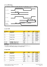
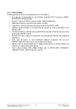
4.4 Test Signal Configuration
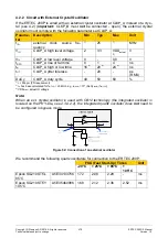
Test Pins
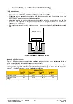
External Wiring in Function Mode
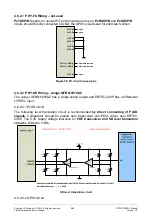
Internal Wiring
TEST
low-impedance to ground (GND)
- pull-down (ca. 50k )
- spike filter < 40 ns
TACT
low-impedance to ground (GND)
- pull-down (ca. 50k )
- spike filter < 40 ns
TAP_SEL
low-impedance to ground (GND)
-
no
pull!
- spike filter < 40 ns
TMC1
straight to ground (GND)
-
no
pull!
- no
spike filter!
TMC2
straight to ground (GND)
-
no
pull!
- no
spike filter!
The module design must comply
strictly
with the external test signal configuration given in
the table.
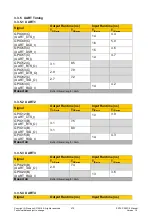
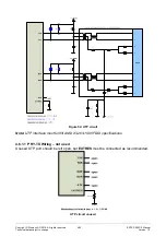
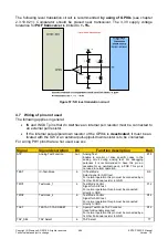
For the module test, the ERTEC 200P can be switched to boundary scan mode by setting
the test signals as shown in the table below:
TACT
TAP_SE
L
TEST
TMC1
TMC2
Description
0
0
0
0
0
Function mode
1
1
0
0
0
ERTEC 200P boundary scan
mode
The boundary scan is controlled over the JTAG interface (see 3.3.8).
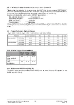
4.5 JTAG Wiring
The JTAG interface is an interface over which the boundary scan register can be con-
trolled or which can be used for ERTEC 200P debugging. The JTAG reset is purposefully
implemented without an internal pull resistor so that various debugger connections are
possible (Hitex or MC). A filter integrated in ERTEC 200P ensures that spikes <= 40 ns
(best case) at JTAG reset XTRST are suppressed (see 4.1.4
. A spike at XTRST is not
usually forwarded to the JTAG controller as this would require a sequence over TDI/TMS
and TCK.
The table below shows the various recommendations for external pull-up/down configura-
tions of the JTAG interface signals.
JTAG
Signal
Signal
Direction
ERTEC 200P
internal pull
(siehe Kap.
Circuit for
Production
(ETB not
accessable
via AHB)
Circuit for
Debugging,
ARM recom-
mended
(ETB
accessable
via AHB)
recommended
JTAG circuit
Recommendation from Debug
supplier (Lauterbach)
XTRST
in
-
10k pulldown
4k7 Pullup
10k Pulldown
default
and 4k7 Pullup
Assembly
option
You should place a pull-down resistor
(1k - 47k) on this signal on target
side, although this is not JTAG
conform. It ensures the on-chip
debug logic is inactive when the
debugger is not connected.
RTCK
in/out
-
not necessary
4k7 Pulldown
4k7 Pulldown
If this is not required, then it can be
used to compensate the propagation
delays on driver and cable. This
allows to reach higher JTAG clock
frequencies. Therefore you need to
feed-back the TCK signal buffered or
unbuffered to this line. On an unbuff-