Semiconductor Group
6-44
1999-04-01
On-Chip Peripheral Components
C541U
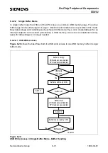
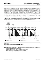
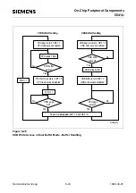
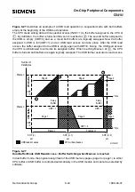
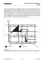
Figure 6-27 describes an example of a USB read operation in sequential mode with both buffers
empty at the beginning of the USB read operation.
The CPU starts writing data with sequential access (INCE=1) to the buffer assigned to the CPU at
. By definition, the buffer is full when MaxLen is reached at
. The second buffer assigned to
the USB is empty (UBF=0) and as a result both buffers are logically swapped. Now the buffer
assigned to USB is full (UBF=1) and an USB read access can take place. After the USB read
access, the buffer assigned to the USB is empty again with UBF=0. During the USB read access
the CPU is still allowed to write into its assigned buffer. When reaching MaxLen at
, the CPU
buffer is full and both buffers are again logically swapped. The USB further execute its read access.
Figure 6-27
Dual Buffer Mode USB Read Access : Buffer Switching when MaxLen is reached
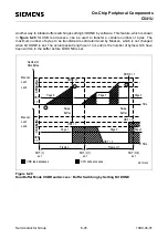
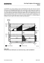
In dual buffer mode, the physical assignment of the USB memory pages (page 0 or page 1) to either
CPU buffer or USB buffer is controlled automatically in the USB module and cannot be selected by
software.
1
2
3
Frame n
Frame n+1
Time
SOF (n)
set
Number of
Data Bytes
MaxLen
USB read accesses
CPU write accesses
MCT03407
SOF (n+2)
set
Time
SOF (n+1)
set
1
3
Page 0
Page 1
Page 1
Page 0
UBF = 0
Swap
Buffer
Swap
Buffer
UBF
= 0
USB Buffer
CPU Buffer
CBF
= 0
MaxLen
Page 0
2
Page 1
UBF = 1
UBF = 1
Summary of Contents for C541U
Page 1: ... 8 LW 026 0LFURFRQWUROOHU 8VHU V 0DQXDO http www siem ens d Sem iconductor ...
Page 7: ......
Page 21: ...Semiconductor Group 2 6 1997 10 01 Fundamental Structure C541U ...
Page 37: ...Semiconductor Group 4 6 1997 10 01 External Bus Interface C541U ...
Page 133: ...Semiconductor Group 6 88 1999 04 01 On Chip Peripheral Components C541U ...
Page 163: ...Semiconductor Group 8 8 1997 10 01 Fail Safe Mechanisms C541U ...
Page 185: ...Semiconductor Group 10 14 1997 10 01 OTP Memory Operation C541U ...

