Semiconductor Group
6-25
1999-04-01
On-Chip Peripheral Components
C541U
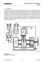
When the SSC is enabled and in master mode, pins P1.3 / SRI, P1.4 / STO, and P1.2 / SCLK will
be switched to the SSC control function. P1.4 / STO and P1.2 / SCLK actively will drive the lines
P1.5 / SLS will remain a regular I/O pin.
The output latches of port pins dedicated to alternate functions must be programmed to logic 1
(= state after reset).
In slave mode all four control pins will be switched to the alternate function. However, STO will stay
in the tristate state until the transmitter is enabled by SLS input being low and the TEN control bit is
set to 1. This allows for more than one slave to be connected to one select line and the final
selection of the slave will be done by a software protocol.
6.3.3 Baudrate Generation (Master Mode only)
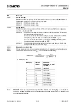
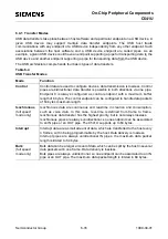
The baudrate clock is generated out of the processor clock (fosc). This clock is fed into a resetable
divider with seven outputs for different baudrate clocks (fosc/4 to fosc/256). One of these eight
clocks is selected by the bits BRS2,1,0 in SSCCON and provided to the shift control logic.
Whenever the shift register is loaded with a new value, the baudrate generation is restarted with the
trailing edge of the write signal to the shift register. In the case of CPHA = 0 the baudrate generator
will be restarted in a way, that the first SCLK clock transisition will not occur before one half transmit
clock cycle time after the register load. This ensures that there is sufficient setup time between MSB
or LSB valid on the data output and the first sample clock edge and that the MSB or LSB has the
same length than the other bits. (No special care is necessary in case of CPHA=1, because here the
first clock edge will be used for shifting).
6.3.4 Write Collision Detection
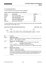
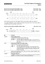
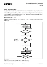
When an attempt is made to write data to the shift register while a transfer is in progress, the WCOL
bit in the status register will be set. The transfer in progress continues uninterrupted, the write will
not access the shift register and will not corrupt data.
However, the data written erroneously will be stored in a shadow register and can be read by
reading the STB register.
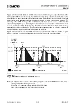
Depending on the operation mode there are different definitions for a transfer being considered to
be in progress:
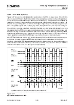
Master Mode :
CPHA=0:
from the trailing edge of the write into STB until the last sample clock edge
CPHA=1:
from the first SCLK clock edge until the last sample clock edge
Note, that this also means, that writing new data into STB immediately after the transfer
complete flag has been set (also initiated with the last sample clock edge) will not generate a
write collision. However, this may shorten the length of the last bit (especially at slow baudrates)
and prevent STO from switching to the forced "1" between transmissions.
Slave Mode :
CPHA=0:
while SLS is active
CPHA=1:
from the first SCLK clock edge until the last sample clock edge
Summary of Contents for C541U
Page 1: ... 8 LW 026 0LFURFRQWUROOHU 8VHU V 0DQXDO http www siem ens d Sem iconductor ...
Page 7: ......
Page 21: ...Semiconductor Group 2 6 1997 10 01 Fundamental Structure C541U ...
Page 37: ...Semiconductor Group 4 6 1997 10 01 External Bus Interface C541U ...
Page 133: ...Semiconductor Group 6 88 1999 04 01 On Chip Peripheral Components C541U ...
Page 163: ...Semiconductor Group 8 8 1997 10 01 Fail Safe Mechanisms C541U ...
Page 185: ...Semiconductor Group 10 14 1997 10 01 OTP Memory Operation C541U ...

