Semiconductor Group
4-3
1997-10-01
External Bus Interface
C541U
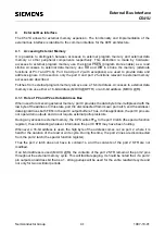
4.1.2 Timing
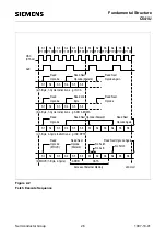
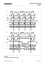
The timing of the external bus interface, in particular the relationship between the control signals
ALE, PSEN, RD, WR and information on port 0 and port 2, is illustated in figure 4-1 a) and b).
Data memory:
in a write cycle, the data byte to be written appears on port 0 just before WR is
activated and remains there until after WR is deactivated. In a read cycle, the
incoming byte is accepted at port 0 before the read strobe is deactivated.
Program memory: Signal PSEN functions as a read strobe.
4.1.3 External Program Memory Access
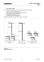
The external program memory is accessed under two conditions:
– - whenever signal EA is active (low); or
– - whenever the program counter (PC) content is greater than 7FFFH
When the CPU is executing out of external program memory, all 8 bits of port 2 are dedicated to an
output function and must not be used for general-purpose I/O. The content of the port 2 SFR
however is not affected. During external program memory fetches port 2 lines output the high byte
of the PC, and during accesses to external data memory they output either DPH or the port 2 SFR
(depending on whether the external data memory access is a MOVX @DPTR or a MOVX @Ri).
4.2
PSEN, Program Store Enable
The read strobe for external program memory fetches is PSEN. It is not activated for internal
program memory fetches. When the CPU is accessing external program memory, PSEN is
activated twice every instruction cycle (except during a MOVX instruction) no matter whether or not
the byte fetched is actually needed for the current instruction. When PSEN is activated its timing is
not the same as for RD. A complete RD cycle, including activation and deactivation of ALE and RD,
takes 6 oscillator periods. A complete PSEN cycle, including activation and deactivation of ALE and
PSEN, takes 3 oscillator periods. The execution sequence for these two types of read cycles is
shown in figure 4-1 a) and b).
4.3
Overlapping External Data and Program Memory Spaces
In some applications it is desirable to execute a program from the same physical memory that is
used for storing data. In the C541U the external program and data memory spaces can be
combined by the logical-AND of PSEN and RD. A positive result from this AND operation produces
a low active read strobe that can be used for the combined physical memory. Since the PSEN cycle
is faster than the RD cycle, the external memory needs to be fast enough to adapt to the PSEN
cycle.
Summary of Contents for C541U
Page 1: ... 8 LW 026 0LFURFRQWUROOHU 8VHU V 0DQXDO http www siem ens d Sem iconductor ...
Page 7: ......
Page 21: ...Semiconductor Group 2 6 1997 10 01 Fundamental Structure C541U ...
Page 37: ...Semiconductor Group 4 6 1997 10 01 External Bus Interface C541U ...
Page 133: ...Semiconductor Group 6 88 1999 04 01 On Chip Peripheral Components C541U ...
Page 163: ...Semiconductor Group 8 8 1997 10 01 Fail Safe Mechanisms C541U ...
Page 185: ...Semiconductor Group 10 14 1997 10 01 OTP Memory Operation C541U ...

