Semiconductor Group
4-1
1997-10-01
External Bus Interface
C541U
4
External Bus Interface
The C541U allows for external memory expansion. The functionality and implementation of the
external bus interface is identical to the common interface for the 8051 architecture.
4.1
Accessing External Memory
It is possible to distinguish between accesses to external program memory and external data
memory or other peripheral components respectively. This distinction is made by hardware:
accesses to external program memory use the signal PSEN (program store enable) as a read
strobe. Accesses to external data memory use RD and WR to strobe the memory (alternate
functions of P3.7 and P3.6). Port 0 and port 2 (with exceptions) are used to provide data and
address signals. In this section only the port 0 and port 2 functions relevant to external memory
accesses are described.
Fetches from external program memory always use a 16-bit address. Accesses to external data
memory can use either a 16-bit address (MOVX @DPTR) or an 8-bit address (MOVX @Ri).
4.1.1 Role of P0 and P2 as Data/Address Bus
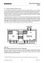
When used for accessing external memory, port 0 provides the data byte time-multiplexed with the
low byte of the address. In this state, port 0 is disconnected from its own port latch, and the address/
data signal drives both FETs in the port 0 output buffers. Thus, in this application, the port 0 pins are
not open-drain outputs and do not require external pullup resistors.
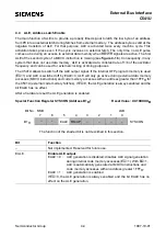
During any access to external memory, the CPU writes FFH to the port 0 latch (the special function
register), thus obliterating whatever information the port 0 SFR may have been holding.
Whenever a 16-bit address is used, the high byte of the address comes out on port 2, where it is
held for the duration of the read or write cycle. During this time, the port 2 lines are disconnected
from the port 2 latch (the special function register).
Thus the port 2 latch does not have to contain 1s, and the contents of the port 2 SFR are not
modified.
If an 8-bit address is used (MOVX @Ri), the contents of the port 2 SFR remain at the port 2 pins
throughout the external memory cycle. This will facilitate paging. It should be noted that, if a port 2
pin outputs an address bit that is a 1, strong pullups will be used for the entire read/write cycle and
not only for two oscillator periods.
Summary of Contents for C541U
Page 1: ... 8 LW 026 0LFURFRQWUROOHU 8VHU V 0DQXDO http www siem ens d Sem iconductor ...
Page 7: ......
Page 21: ...Semiconductor Group 2 6 1997 10 01 Fundamental Structure C541U ...
Page 37: ...Semiconductor Group 4 6 1997 10 01 External Bus Interface C541U ...
Page 133: ...Semiconductor Group 6 88 1999 04 01 On Chip Peripheral Components C541U ...
Page 163: ...Semiconductor Group 8 8 1997 10 01 Fail Safe Mechanisms C541U ...
Page 185: ...Semiconductor Group 10 14 1997 10 01 OTP Memory Operation C541U ...

