Semiconductor Group
6-78
1999-04-01
On-Chip Peripheral Components
C541U
6.4.8.5
Register Set
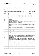
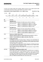
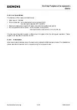
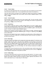
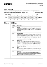
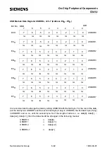
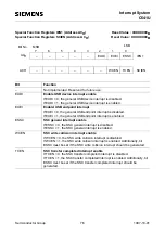
A set of control and data registers are defined for the USB module in low speed operation.
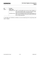
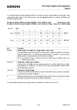
USB Module Control Register USBDCR (Address E7H)
Reset Value : 00H
Bit
Function
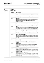
TYPE3 - 0
Transfer Type
MSB
LSB
USBDCR
7
6
5
4
3
2
1
0
Bit No.
E7H
rw
rw
LEN0
LEN1
rw
LEN2
LEN3
TYPE0
TYPE1
TYPE2
TYPE3
rw
rw
rw
rw
rw
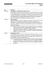
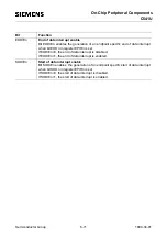
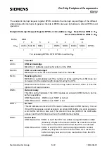
TYPE3 - 0
Description
0000
Empty
Software is required to write this value to generate an
acknowledgement and trigger the next activity in the
hardware.
0001
Reserved
0010
SETUP packet
A SETUP packet has been received and the setup data is
stored in the USBDRn registers and SETUP interrupt request
is also generated. A read operation to register USBDCR
resets the pending interrupt request, while TYPE bit field
maintains its current value (0010
B
).
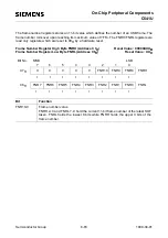
0011
OUT packet
An OUT packet has been received by endpoint zero and is
stored in the USBDRn registers and OUT interupt request is
generated. A read operation to register USBDCR resets the
pending interrupt request, while TYPE bit field maintains its
current value (0011
B
).
0100
Stall
The module is stalled including control endpoint and both
interrupt endpoints.
0101
IN packet
An IN packet has been set up for endpoint zero, which is
directed to the host. Software is required to write this value to
trigger the data packet to be sent to the host.
Summary of Contents for C541U
Page 1: ... 8 LW 026 0LFURFRQWUROOHU 8VHU V 0DQXDO http www siem ens d Sem iconductor ...
Page 7: ......
Page 21: ...Semiconductor Group 2 6 1997 10 01 Fundamental Structure C541U ...
Page 37: ...Semiconductor Group 4 6 1997 10 01 External Bus Interface C541U ...
Page 133: ...Semiconductor Group 6 88 1999 04 01 On Chip Peripheral Components C541U ...
Page 163: ...Semiconductor Group 8 8 1997 10 01 Fail Safe Mechanisms C541U ...
Page 185: ...Semiconductor Group 10 14 1997 10 01 OTP Memory Operation C541U ...

