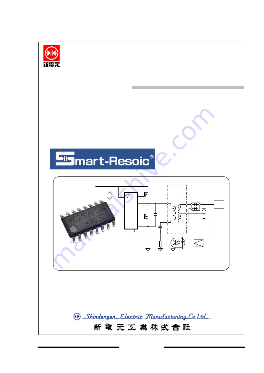
MCZ5207SG
SHINDENGEN
ELECTRIC MFG.CO.,LTD
- 1 -
CAT.No. 1H0100-1E
MCZ5207SG APPLICATION NOTE
Jan.2013 Ver1.0
LLCCurrent resonant bridgecontroller
+
Vo1
Page 1: ...MCZ5207SG SHINDENGEN ELECTRIC MFG CO LTD 1 CAT No 1H0100 1E MCZ5207SG APPLICATION NOTE Jan 2013 Ver1 0 LLC Current resonant bridge controller MCZ5207SG Vo1...
Page 2: ...for a long period under continuous operation please make sure to consult us in advance Caution Caution Caution Caution Caution Do not attempt under any conditions to repair or modify IC products by y...
Page 3: ...t protection Vsen 2 3 4 Current peak limiting fast OCP CS1 2 3 5 Fequency clamped slow OLP CS2 CSO 2 3 6 Capacitive mode protection CS2 2 3 7 Safe startup 2 3 8 Soft start SST 2 3 9 Timer delayed latc...
Page 4: ...direct gate driver 2 Optimized protections OCP burst Timer delayed latch Thermal for LLC converter 3 Bidirectional resonant current sensing 4 Bidirectional capacitive mode protection 5 Vcc supply up...
Page 5: ...FF SST Latch OCP1 OCP Counter 8 times LLC STOP Control Logic Burst ON OFF High Voltage Driver Dropper AS OFF FB discharge SS Reset SS st sp Counter reset Vss Reset Latch Stop S Q R S Soft Start Timer...
Page 6: ...or Output Averaged OLP response is determined 7 CS1 Current Sensing input for shorted load protection Peak current limiting sensing threshold voltage is 0 5V 8 CS2 Current Sensing input for frequency...
Page 7: ...CZ5207SG SHINDENGEN ELECTRIC MFG CO LTD 7 1 5 Applicable circuit configuration Most simple SEPP Single Ended Push Pull Input ripple current reduction Half Bridge For high power application Full Bridge...
Page 8: ...rive VDD Vc2 Vc2 terminal is an output of internal 10 2V dropper for the gate driver Vc2 output is also a voltage source of boot strapping high side VDD Filtering capacitor should be placed close to V...
Page 9: ...tching or SBD is recommended like D1NS4 40V axial SBD or M1FM3 30V SMD SBD 2 3 2 Oscillator FB The timing of gate drive pulse VGL and VGH is determined by charging and discharging time period of timin...
Page 10: ...bus voltage increasing condition Csst starts to be charged when Vsen terminal voltage reaches to Vsen1 ss reset 3 55V and Gate output is enabled when SST terminal voltage reaches to Vss st 0 6V Opera...
Page 11: ...en heavy non ZVS surge current cannot trigger OCP1 From OCP1 detection to Ct charging has 200nsec time delay due to internal filter 2 3 5 Frequency clamped averaging OLP CS2 and CSO The MCZ5207SG has...
Page 12: ...k 4 4V Even if CS2 terminal voltage crosses this threshold during this time period anti capacitive mode protection does not work Timer delayed latching protection is enabled only when LLC is operating...
Page 13: ...atching protection timing capacitor SST terminal capacitor Csst starts to be charged in two condition as following 1 OCP1 or OCP2 operates continuously OR 2 Anti capacitive mode protection operates in...
Page 14: ...sirable latching When abnormal condition is counted twice IC enters into latched stop mode 2 3 10 Boot strapping circuit High side floating VDD VB VS capacitor is charged during conduction period of l...
Page 15: ...MCZ5207SG SHINDENGEN ELECTRIC MFG CO LTD 15 Np Dboot Cboot 0 1 uF 16V D1NK60 D1FK60 Vc2 PGND MCZ5207SG VB VS VGH VGL Fig 14 Boot Strapping circuit...
Page 16: ...tage is 2 5V Circuit configuration is shown in Fig 15 When AS signal is not applied Vas open 2 5V VGH and VGL output is symmetrically 50 duty cycle and if AS terminal is pulled down externally to less...
Page 17: ...d to 1 0V on 0 9V off preparing to PFC stopped LLC operation Operation will recover to normal continuous operation when AS terminal voltage decreases to 3 0V or less Fig 18 BURST w external signal con...
Page 18: ...000pF between Vsen and GND for filtering Low side resistor RvsenseL init is obtained from formula 1 Correct value of Vbulkreset threshold is obtained from formula 2 using actual value of RvsenseL In A...
Page 19: ...istance Minimum frequency fmin is determined by Rt value Connect between FB and GND Relation between Rt resistance and frequency is shown in characteristic specification sheet The estimated value of f...
Page 20: ...ependent sensing and b shows CS1 2 common sensing connection Generally OCP2 operating point is lower than OCP1 s In this condition OCP2 stabilizes LLC operating frequency in transient over load peak l...
Page 21: ...ut Fig 21 OLP characteristics example Cr Cr a CS1 2 independent sensing b CS1 2 common sensing Fig 20 CS1 and CS2 current sensing circuit 13 12 11 det 2 1 2 1 2 1 det 2 1 2 1 det A 0 5 R R R R I ohm 0...
Page 22: ...MCZ5207SG SHINDENGEN ELECTRIC MFG CO LTD 22 4 Circuit diagram 4 1 Configuration example of DC to DC dual output LLC...
Page 23: ...MCZ5207SG SHINDENGEN ELECTRIC MFG CO LTD 23 5 Dimension 5 1 SOP16 MCZ5207SG...
Page 24: ...MCZ5207SG SHINDENGEN ELECTRIC MFG CO LTD 24 Notes...