


UX-P115U
5 – 12
[4] Circuit description of power supply PWB
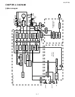
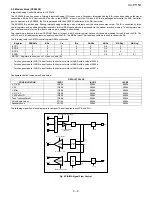
1. Block diagram
2. Noise filter circuit
The input noise filter section is composed of L1 and C1, which reduces
normal mode noise from the AC line and common mode noise to the
AC line.
3. Rectifying/smoothing circuit
The AC input voltage is rectified by diode D1, 2, 3, 4 and smoothed by
capacitor C2 to supply DC voltage to the switching circuit section.
4. SWitching circuit
This circuit includes MOS FET Q1 and the gate drive circuit, and com-
ponents around Q1.
In this circuit, the DC voltage supplied from the rectifying/smoothing
section is converted into high Frequency pulses by ON/OFF repetition
of Q1.
5. Control circuit
This circuit controls output voltage of +24V by adjusting ON period of
Q1, looking at signal from photo coupler PC1.
In this operation PC1 takes charge of important part.
The over current protection is performed by bringing Q1 to OFF state
through detection of voltage of T1 subwinding.
The over voltage protection is performed by operating the over current
protection circuit through detection of Zener diode ZD4 and short-cir-
cuiting of load.
[5] Circuit description of CIS unit
1. CIS
CIS is an image sensor which puts the original paper in close contact
with the full-size sensor for scanning, being a monochromatic type with
the pixel number of 1,728 dots and the main scanning density of 8
dots/mm.
It is composed of sensor, rod lens, LED light source, light-conductive
plate, control circuit and so on, and the reading line and focus are pre-
viously adjusted as the unit.
Due to the full-size sensor, the focus distance is so short that the set is
changed from the light weight type to the compact type.
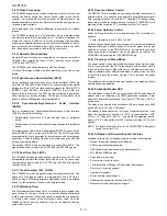
2. Waveforms
The following clock is supplied from SCE209 of the control board, and
VO is output.
Noise
Filter
Circuit
Rectifying
Smoothing
Circuit
Switching
Circuit
+5V
+24V
AC IN
Photo Coupler
F1
3.15A/125V
F3
4A/32V
Control
Circuit
Fig. 7
Fig. 8
5ms
2µs
0V
0.8V~2.9V
(White original paper)
Approx.3.3V
Φ
T
CISCLK
VO