28
28
Development Kit
28
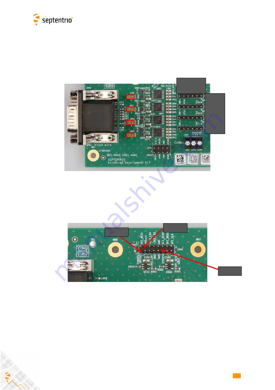
Alternatively, 3.3V TTL signals are available through four 6-pin headers, as shown below.
The pinout is compatible with standard FTDI 6-pin SIL connectors. To route a COM port to
the 6-pin header instead of the BD9 connector, a jumper must be placed on J800 (COM1),
J801 (COM2), J804 (COM3) and/or J805 (COM4). Only those COM ports for which the
jumper is placed are routed to the 6-pin header. The other COM ports are still routed to
the DB9 connectors, using the RS232 levels.
Note that, when using the DB9 connectors, the baud rate must not be larger than
230400baud. This limitation does not apply to the TTL signals.
4.6
PPS Out and Event Inputs
The PPSout pin of header J500 is directly connected to the PPS1 pin of the AsteRx-m3 (see
section 2.5.1). The PPS level is 3.3V.
The EVENTA and EVENTB pins of J500 are connected to the EventA and EventB pins of the
AsteRx-m3 through a buffer. The voltage level at the header pins must be between -0.5V
and +6V. These pins are pulled-down by a 100kOhm resistor. See section 2.8 for more
details.
Note that the second PPS pin of the OEM module (PPS2) is not exposed in the DevKit.
EVENTB
EVENTA
PPSOUT
COM1
COM2
COM3
COM4
G
ND
R
TS (O)
NC
R
X (I)
TX
(O)
C
TS (
I)


