background image

Pickup device:

 1/4”

Effective pixels:

 752 (H) x 582 (V)

Horizontal resolution:

 Over 520 TV lines

Lens:

 22 power zoom lens, f=4.0-88 mm (F1.6-3.8),

          Electronic zoom and gearing, Zoom speed setting possible

Electronic zoom:

 16 power (combined with optic zoom gives 352 power max)

                              Max zoom magnification setting possible, Vertical resolution ON/OFF setting

Autofocus:

 AUTO/MANUAL, AF area setting possible (3 step)

Iris control:

 AUTO/MANUAL, 1/2 EV steps

Synchronization method:

 Internal synchronization/Line lock, V phase adjustment possible

Lowest image illumination:

 2.0 lx (F 1.6) at max AGC gain

                                               0.06 lx (F 1.6) at x32 electronic sensitivity boost

S/N:

 Over 48dB

Backlight compensation:

 Multi-spot evaluative metering

                                            5 spot centerweighted average metering, 48 multi-spot metering

Electric shutter: 

 Fast shutter speed mode (SHORT);

                               1/50, 1/120, 1/250, 1/500, 1/1000, 1/2000, 1/4000, 1/10000


 Slow shutter speed mode (LONG); x1, x2, x4, x8, x16, x32

Electronic sensitivity boosting:

 AUTO/OFF, works with auto iris, Up to x32 max setting possible

White balance:

 ATW/AWC/MWB

AGC gain:

 ON allows selection of 

±

0dB, +6dB, +9dB, -6dB

                   OFF allows manual adjustment from 0dB to 30dB

Motion detector:

 ON/OFF, ON allows setting of detection patterns on a 48 zone screen for

                             6 motion settings (size, masking, sensitivity, zoom, interval, alarm sign)

Privacy masking:

 ON/OFF, max of 4 masked locations, Password lock possible

Alarm input/output (back panel control terminals):

 Alarm input: 1 (for external alarm switch)

               Alarm output: 1 (for sending a signal to the system controller or an alarm
                                     detection device such as a buzzer)

Mirror image effect:

 Horizontally (H), vertically (V), horizontally and vertically (HV)

Camera ID:

 ON/OFF, 16 characters

View settings:

 9 (0-8) screen files can be established, and each file can set

                         7 capturing characteristics such as iris

Communications:

 Coaxial control, RS-485

Operational temperature/humidity:

 -10 - 50 

°

C/below 90 %RH

Power source:

 24 V AC, 50 Hz/12-15 V DC, 

Power consumption:

 4.5 W, 

Weight:

 380 g

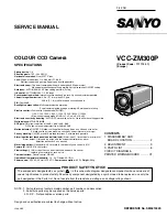
SERVICE MANUAL

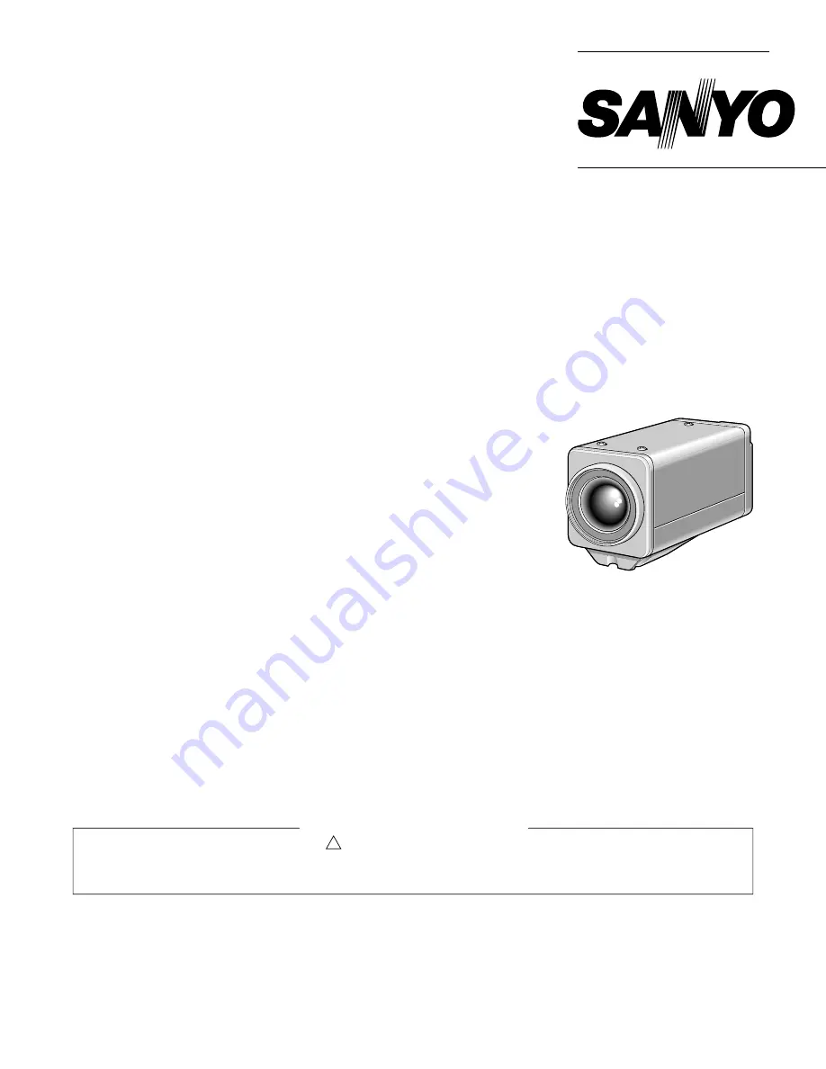
COLOUR CCD Camera

VCC-ZM300P

(Product Code : 117 113 01)
(Europe)

FILE NO.

REFERENCE No. SM5310420

L5AA2/XE

NOTE : 1. Parts order must contain model number, part number, and description.
             2. Substitute parts may be supplied as the service parts.
             3. N. S. P. : Not available as service parts.

Design and specification are subject to change without notice.

The components designated by a symbol (   !   ) in this schematic diagram designates components whose value are of

special significance to product safety. Should any component designated by a symbol need to be replaced, use only the

part designated in the Parts List. Do not deviate from the resistance, wattage, and voltage ratings shown.

PRODUCT SAFETY NOTICE

CONTENTS

1. DISASSEMBLY AND
    BOARD LOCATION ....................... 2
2. ADJUSTMENT ............................... 3
3. PARTS LIST ................................... 6
CIRCUIT DIAGRAM &
PRINTED WIRING BOARDS ........... C1

SPECIFICATIONS

Summary of Contents for VCC-ZM300P

Page 1: ...y masking ON OFF max of 4 masked locations Password lock possible Alarm input output back panel control terminals Alarm input 1 for external alarm switch Alarm output 1 for sending a signal to the system controller or an alarm detection device such as a buzzer Mirror image effect Horizontally H vertically V horizontally and vertically HV Camera ID ON OFF 16 characters View settings 9 0 8 screen fi...

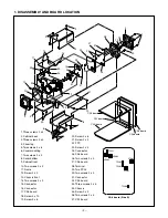
Page 2: ...crew 3 x 10 19 Screw 3 x 6 20 Screw 3 x 6 21 Screw 2 x 3 22 FPC 23 Screw 2 x 3 24 Connector 25 CA4 board 26 Two screws 2 x 3 27 CA5 board 28 Terminal 29 Two FPCs 30 Two screws 2 x 3 31 Connector 32 CA2 board 33 Three screws 2 x 5 34 Chassis 35 Screw 2 x 3 36 Two screws 2 x 5 37 CA1 board CA1 board CA2 board CA3 board CA4 board CA5 board 1 2 3 3 4 5 6 7 8 9 10 11 12 13 14 16 17 15 18 19 20 21 23 24...

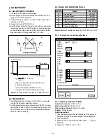
Page 3: ...ure frame size becomes as shown below when performing the adjustment with the gray scale chart ITE gray scale chart γ 0 45 2 2 PREPARATION 1 Install the adjustment software VHJ 0140 in a computer running the Windows operating system 2 Use the adjustment commander relay jig VHJ 0142 to con nect CN204 of side B in the CA 2 board and serial port RS 232C of computer and then turn on the power for the ...

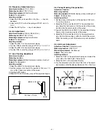
Page 4: ...4 When AUTO ADJ NG display carry out the adjustment again 2 8 Privacy Masking Compensation Adjustment location Measuring location Measuring equipment Monitor display privacy masking chart Subject No designation Adjusting method 1 Set the privacy masking chart at the position of 940 mm 10 mm from the lens 2 Select the TELE under the LENS T in the adjustment dis play Adjust the field angle so that t...

Page 5: ...t the R and B in the adjustment display Adjust by oper ating key of a keyboard so that the white luminescent spot is the center of the vectorscope 3 Select the R GAIN R HUE B GAIN and B HUE in the ad justment display Adjust by operating level scroll bar so that the red and yellow luminescent spots are the size and po sition which are designated in the vectorscope 4 Select the ROM CLEAR in the adju...

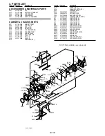
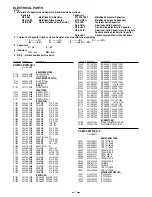
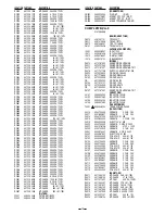
Page 6: ...505 645 050 3740 OPTICAL FILTER 7506 613 197 8355 ASSY UNIT CCD PAL 7507 645 053 7639 TERMINAL PWB 2P CN515 CA1 613 198 6541 COMPL PWB CA 1 CA2 613 198 6572 COMPL PWB CA 2 CA3 613 198 6558 COMPL PWB CA 3 CA4 613 198 6596 COMPL PWB CA 4 CA5 613 198 6602 COMPL PWB CA 5 NJ510 411 126 4702 SCR PAN SW W 3X6 NJ520 412 051 6007 SPECIAL SCREW 3X4 NJ530 411 021 5705 SCR S TPG BIN 3X6 NJ540 411 030 5406 SCR...

Page 7: ...3 155 1807 CERAMIC 0 01U K 25V C1118 403 285 4808 TA SOLID 3 3U M 20V C1125 403 164 0204 CERAMIC 0 1U Z 25V C1134 403 285 4808 TA SOLID 3 3U M 20V C1135 403 164 0204 CERAMIC 0 1U Z 25V C1136 403 285 4808 TA SOLID 3 3U M 20V C1137 403 164 0204 CERAMIC 0 1U Z 25V C1138 403 285 3603 TA SOLID 4 7U M 6 3V C1139 403 164 0204 CERAMIC 0 1U Z 25V RESISTORS R1001 401 105 7909 MT GLAZE 0 000 ZA 1 16W R1002 4...

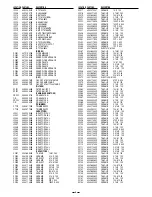
Page 8: ...M 25V C2019 403 285 6802 TA SOLID 10U M 6 3V C2020 403 346 2309 CERAMIC 0 1U K 10V C2021 403 285 6802 TA SOLID 10U M 6 3V C2022 403 311 4505 CERAMIC 1000P K 50V C2023 403 311 4505 CERAMIC 1000P K 50V C2024 403 309 8409 CERAMIC 10P D 50V C2026 403 285 4006 TA SOLID 4 7U M 10V C2027 403 346 2309 CERAMIC 0 1U K 10V C2028 403 346 2309 CERAMIC 0 1U K 10V C2040 403 285 3603 TA SOLID 4 7U M 6 3V C2049 40...

Page 9: ...W R2070 401 226 1503 MT GLAZE 0 000 ZA 1 16W R2071 401 224 9303 MT GLAZE 1K JA 1 16W R2072 401 225 1405 MT GLAZE 47K JA 1 16W R2073 401 225 1405 MT GLAZE 47K JA 1 16W R2074 401 225 3805 MT GLAZE 1 5K JA 1 16W R2075 401 225 0200 MT GLAZE 3 3K JA 1 16W R2076 401 225 0309 MT GLAZE 33 JA 1 16W R2077 401 224 8900 MT GLAZE 100K JA 1 16W R2080 401 225 1405 MT GLAZE 47K JA 1 16W R2082 401 226 1503 MT GLAZ...

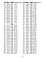
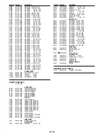
Page 10: ... MT GLAZE 0 000 ZA 1 16W R2422 401 226 1503 MT GLAZE 0 000 ZA 1 16W R2450 401 225 0606 MT GLAZE 5 6K JA 1 16W R2451 401 224 8900 MT GLAZE 100K JA 1 16W R2452 401 225 0606 MT GLAZE 5 6K JA 1 16W R2453 401 224 8900 MT GLAZE 100K JA 1 16W R2454 401 225 0309 MT GLAZE 33 JA 1 16W R2456 401 225 1603 MT GLAZE 390 JA 1 16W R2457 401 225 1603 MT GLAZE 390 JA 1 16W FILTERS F2001 645 006 3404 FILTER EMI 470P...

Page 11: ...Z 10V C4090 403 113 3805 CERAMIC 1000P K 50V C4091 403 155 1807 CERAMIC 0 01U K 25V C4092 403 175 4505 ELECT47U M 6 3V C4093 403 162 4709 ELECT10U M 16V C4094 403 155 1807 CERAMIC 0 01U K 25V C4095 403 175 4505 ELECT47U M 6 3V C4096 403 155 1807 CERAMIC 0 01U K 25V C4097 403 155 1807 CERAMIC 0 01U K 25V C4098 403 162 4709 ELECT10U M 16V C4099 403 155 1807 CERAMIC 0 01U K 25V C4101 403 164 0204 CER...

Page 12: ... VARISTOR NV047D07 VA511 645 045 7449 SURGE ABSORBER VA512 645 045 7449 SURGE ABSORBER VA514 645 045 7449 SURGE ABSORBER VA515 645 045 7449 SURGE ABSORBER DIODES D5001 407 065 3906 LED SLP 135B 51 D5002 407 206 5400 ZENER DIODE UDZS8 2B D5003 407 206 5400 ZENER DIODE UDZS8 2B D5011 407 206 5400 ZENER DIODE UDZS8 2B D5015 407 222 6306 ZENER DIODE UDZS3 9B D5016 407 222 6306 ZENER DIODE UDZS3 9B D50...

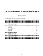
Page 13: ...BLOCK DIAGRAM C4 CA 1 CIRCUIT C5 IC101 IC102 IC103 BLOCK DIAGRAMS C6 CA 1 CIRCUIT WAVEFORMS CA 2 CIRCUIT WAVEFORMS CA 2 CIRCUIT C7 CA 3 CIRCUIT C10 IC313 BLOCK DIAGRAM CA 4 CIRCUIT C11 CA 5 CIRCUIT C12 PRINTED WIRING BOARDS P W B CA 1 BOARD SIDE A B C13 CA 2 BOARD SIDE A B CA 3 BOARD SIDE A B C14 CA 4 BOARD SIDE A B CA 5 BOARD SIDE A B C15 ...

Page 14: ...HOSE VALUE ARE OF SPECIAL SIGNIFICANCE TO PRODUCT SAFETY SHOULD ANY COMPONENT DESIGNATED BY A SYMBOL NEED TO BE REPLACED USE ONLY THE PART DESIGNATED IN THE PARTS LIST DO NOT DEVIATE FROM THE RESISTANCE WATTAGE AND VOLT AGE RATINGS SHOWN PAL C EX EXPLANATORY NOTES EXAMPLES Resistor 10K 1 16J means 10kilo ohm 5 1 16watt max 1M 1 10K means 1mega ohm 10 1 10watt max Capacitor 0 047 F means 0 047micro...

Page 15: ...A B C D E F G H I J K 1 2 3 4 5 6 7 8 9 10 11 12 13 14 15 16 17 18 19 A B C D E F G H I J K C3 OVERALL WIRING BLOCK DIAGRAM CIRCUIT DIAGRAMS OVERALL WIRING ...

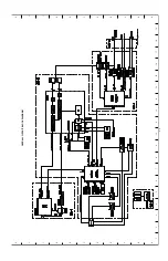
Page 16: ...A B C D E F G H I J K 1 2 3 4 5 6 7 8 9 10 11 12 13 14 15 16 17 18 19 A B C D E F G H I J K C4 OVERALL CIRCUIT BLOCK DIAGRAM ...

Page 17: ...A B C D E F G H I J K 1 2 3 4 5 6 7 8 9 10 11 12 13 14 15 16 17 18 19 A B C D E F G H I J K C5 CA 1 CIRCUIT ...

Page 18: ...AVEFORM TEST POINT LOCATION IC101 1 2V div 20µs div V4 IC101 2 5V div 20µs div V3 IC101 3 5V div 20µs div V2 IC101 12 2V div 50ns div RG IC103 43 2V div 20µs div VD IC101 13 2V div 50ns div H1 IC101 14 2V div 50ns div H2 IC103 44 2V div 10ms div HD IC101 4 5V div 20µs div V1 WF CA1 L54W2US IC103 29 0 5V div 10µs div CCD IN CA 1 CIRCUIT WAVEFORMS TEST POINT LOCATION WAVEFORM IC215 7 200mV div 10µs ...

Page 19: ...A B C D E F G H I J K 1 2 3 4 5 6 7 8 9 10 11 12 13 14 15 16 17 18 19 A B C D E F G H I J K C7 CA 2 CIRCUIT ...

Page 20: ...A B C D E F G H I J K 1 2 3 4 5 6 7 8 9 10 11 12 13 14 15 16 17 18 19 A B C D E F G H I J K C8 CA 2 CIRCUIT LEFT ...

Page 21: ...A B C D E F G H I J K 1 2 3 4 5 6 7 8 9 10 11 12 13 14 15 16 17 18 19 A B C D E F G H I J K C9 CA 2 CIRCUIT RIGHT ...

Page 22: ...A B C D E F G H I J K 1 2 3 4 5 6 7 8 9 10 11 12 13 14 15 16 17 18 19 A B C D E F G H I J K C10 CA 3 CIRCUIT OUT GND V CC CTL C 1 8 6 3 5 REFERENCE VOLTAGE IC313 BLOCK DIAGRAM BA00BC0WF ...

Page 23: ...A B C D E F G H I J K 1 2 3 4 5 6 7 8 9 10 11 12 13 14 15 16 17 18 19 A B C D E F G H I J K C11 CA 4 CIRCUIT ...

Page 24: ...A B C D E F G H I J K 1 2 3 4 5 6 7 8 9 10 11 12 13 14 15 16 17 18 19 A B C D E F G H I J K C12 CA 5 CIRCUIT ...

Page 25: ...A B C D E F G H I J K 1 2 3 4 5 6 7 8 9 10 11 12 13 14 15 16 17 18 19 A B C D E F G H I J K C13 PRINTED WIRING BOARDS P W B CA 1 BOARD SIDE A CA 1 BOARD SIDE B CA 2 BOARD SIDE A CA 2 BOARD SIDE B ...

Page 26: ...A B C D E F G H I J K 1 2 3 4 5 6 7 8 9 10 11 12 13 14 15 16 17 18 19 A B C D E F G H I J K C14 CA 3 BOARD SIDE A CA 3 BOARD SIDE B CA 4 BOARD SIDE A CA 4 BOARD SIDE B ...

Page 27: ...A B C D E F G H I J K A B C D E F G H I J K 1 2 3 4 5 6 7 8 9 C15 CA 5 BOARD SIDE A CA 5 BOARD SIDE B ...

Page 28: ...May 02 SANYO Electric Co Ltd Osaka Japan ...

Reviews: