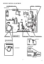
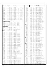
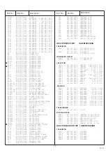
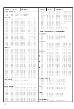
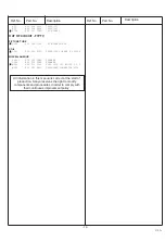
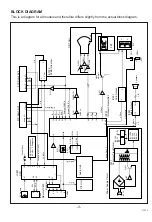
background image

-4-

F7PTV

1. POWER SUPPLY

The power supply circuit of the EB4-A chassis is

composed of a rectifier smoothing circuit, an oscillation
circuit, a control circuit and an output rectifier circuit. The
AC input voltage is full-wave rectified by the rectifier
smoothing circuit, and an unstable DC voltage is
generated at both terminals of the smoothing capacitor
C607. This voltage is input to the oscillation circuit. The
oscillation circuit is provided with a blocking  oscillator
circuit that switches the switching transistor Q613 ON
and OFF, and an oscillation frequency and a duty square
wave pulse are generated in the input windings
according to operation of the control circuit. A square-
wave pulse whose size is dependent on the turn ratio of
the input and output windings is obtained in the output
winding. This is rectified in the output rectifier circuit, and
the desired DC voltage is obtained.

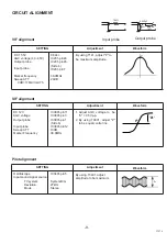
2. IF & DEFLECTION (TDA8361)

The IF output signal from the tuner passes through the

SAW filter, and it is input to pin45 and pin46 of IC201.
The signal input to the IC passes through the IF
amplifier, video detection and video amplifier circuits and
is output from pin7 as a composite video signal. And
after this signal is converted to impedance at Q151,
supplies to the video and chroma amplifier stages. 
The sync.-separation circuit separates the video signals
applied to pin13(internal video signal) or pin15(external
video signal) to vertical- and horizontal-sync. signals
respectively. The horizontal oscillator requires no
external components and is fully integrated. The
oscillator is always running when the start-pin36 is
supplied with 8V. Horizontal drive signal is output from
pin37. VR361 is for adjustment of the horizontal centring.
The separated vertical-sync. signal from sync. separation
circuit passes through the vertical-separation circuit, and
applied to trigger divider circuit. The horizontal oscillation
pulse and input vertical sync. pulse are monitored by the
trigger divider circuit, and switching 50Hz and 60Hz
system, the vertical amplitude automatically adjusted for
50Hz and 60Hz. The output signal from the trigger
divider is triggered  vertical oscillation circuit consisting of
C351, R352 and pin42, and vertical drive pulse is output
from pin43. VR501 is for changing the amount of AC
feedback applied to pin41 and for adjustment of the
vertical amplitude. 

3. VIDEO CHROMA & R.G.B. (TDA8361)

The composite video signal output from the pin7 of

IC101 passes through Q151-Q154, and it is supplied to
pin13. The external video signal output from SCART is
supplied to pin15. The video signal input to pin13 or
pin15 is separated to luminance (Y) signal and chroma
signal in IC201. These pins are used in common with
H/V-sync. separation input. The peaking of Y signal is
adjusted by DC voltage of pin14. (“SHARPNESS”

control) The chroma signal is divided into R-Y and B-Y
chroma signals, demodulated in IC201, and output from
pin30 (R-Y) and pin31 (B-Y). These chroma signals pass
through the 1H delay line circuit (IC271), and they are
input to pin29 (R-Y) and pin28 (B-Y). These R-Y/B-Y
signals pass through RGB matrix circuit and RGB
selector circuit of IC101. The internal RGB signals are
generated in RGB matrix circuit and the RGB selector,
consisting linear amplifiers, clamps and selects either the
internal RGB signals or the external RGB signals input
from pin22(R), pin23(G), pin24(B). Selection is controlled
by the voltage at the RGB switch control (pin21) and
mixed RGB modes are possible since RGB switching is
fast. The RGB switch also functions as a fast blanking
pin by blanking the RGB output stages; here internal and
external RGB signals are overruled. The colour gain is
controlled by DC voltage of pin26. (“COLOUR” control)
The contrast control voltage present at pin25, and the
brightness control voltage present at pin17 controls DC
level of RGB signals. The RGB signals are finally
buffered before being available at the RGB output pins
[pin20 (R), pin19 (G), pin18 (R)].

4. AUDIO OUTPUT(TDA7263M)

The audio signals output from the audio unit are input to

pin1(L) and 5(R) of IC171 and passes through the pre-
amplifier circuit and drive circuit, after which it is input to
the audio amplifier. The audio amplifier is an SEPP
(single-ended, push-pull) OTL type and output to pin8(R)
and 10(L) to directly drive the speakers.

5. VERTICAL OUTPUT (LA7832/LA7832)

An IC (LA7832/LA7833) is used for the vertical output

circuit in this chassis. The vertical drive pulse from pin43
of IC201 is input to pin4 of IC501. This pulse drives
IC501, and vertical scanning is performed. In the first half
of scanning a deflecting current is output from pin2 and
passes through the following path:
Vcc(B4) 

D501 

pin3 

pin2 

DY 

C512 

VR501/R509. An electric charge is then stored in C512.
In the last half of scanning the current path is C512 

DY 

➞ 

pin2 

pin1 

➞ 

VR501/R509 

C512. In this way,

an amplifying sawtooth waveform current flows directly to
DY to perform electron beam defection. Next, in the first
half of the banking period the vertical drive pulse
suddenly becomes OFF, and in order to reduce the
current flowing to DY, the current path becomes as
follows by the inductance of DY:
DY 

pin2 

pin1 

VR501/R509 

C512 

DY. Also,

when the charge of DY has dissipated, the current path
becomes Vcc24V 

pin6 

pin7 

➞ 

C502 

pin3 

pin2

DY 

C512 

➞ 

VR501/R509, and when the

prescribed current value is reached, the vertical drive
pulse becomes ON. This completes one cycle.

CIRCUIT DESCRIPTION

Summary of Contents for CE25B3-C

Page 1: ...net back of the TV set Note This TV receiver will not work properly in foreign countries where the television transmission system and power source differ from the design specifications Refer to the specifications for the design specifications CE25B3 C Contents Safety precautions Specifications 2 Block diagram 3 Cabinet description 4 5 Circuit disassembly 6 Service control adjustment 7 8 Circuit al...

Page 2: ...nly parts designated on the parts list in this manual be used for component replacement designated by mark No deviations from resistance wattage or voltage ratings may be made for replacement items designated by mark 1 An isolation transformer should be connected in the power line between the receiver and the AC line when a service is performed on the primary of the converter transformer of the se...

Page 3: ...8 2 3 4 5 2 Bright 3 Contranst 4 Colour 5 Sharpness Control Keys 10 VL VH U IF TU 1 16 45 46 28 29 30 31 41 48 37 18 19 20 7 13 15 21 22 23 24 X131 SAW Filter IC271 1H Delay R Y B Y R Y B Y CVBS In Functuin In AV1 AV2 11 12 14 16 B G R BLK External CVBS in Internal CVBS in Q151 Q152 Q154 H Drive Q431 Q432 H Outpit V Drive V Feedback Audio In Speakers VR501 C512 H V HV Q2601 Q2611 Q2621 Q171 1 6 3 ...

Page 4: ...pin13 or pin15 is separated to luminance Y signal and chroma signal in IC201 These pins are used in common with H V sync separation input The peaking of Y signal is adjusted by DC voltage of pin14 SHARPNESS control The chroma signal is divided into R Y and B Y chroma signals demodulated in IC201 and output from pin30 R Y and pin31 B Y These chroma signals pass through the 1H delay line circuit IC2...

Page 5: ... base of Q462 to compensate for width variations due to variations in the beam current 7 CPU System and Teletext Control Pin description Pin1 Tuning voltage output Pin2 Brightness control output 6 bit DAC Pin3 Contrast control output 6 bit DAC Pin4 Colour control output 6 bit DAC Pin5 Sharpness control output 6 bit DAC Pin6 Not used GND Pin7 Not used GND Pin8 Power ON OFF output H ON Pin9 AFT sign...

Page 6: ... 6 F7PTV CABINET DISASSEMBLY CABINET BACK DISASSEMBLY 1 Remove 7 screws A 2 Pull out the cabinet back A A A A A A A ...

Page 7: ...361 H Centre VR131 AGC T101 T102 VC141 T141 IC810 Band SW Audio Board SIF Board A101 Tuner IC1202 Int Ext SW IC1201 AV2 SW TP E TP D IC802 Memory IC801 CPU IC001 Audio output Video input Audio input R Headphones Audio input L B1 POWER SUPPLY ADJ TU AGC ADJ AFT ADJ GREY SCALE ADJ FOCUS ADJ MAIN BOARD HIGH VOLTAGE H WIDTH ADJ V CENTRE ADJ H CENTRE ADJ V SIZE ADJ Q641 Q621 Q601 Q611 VR611 R BIAS VR62...

Page 8: ...he Prog on the TV front panel Press the Function button on the Remote control until SCREEN is highlighted This sets up a horizontal scanning line 6 Set screen VR so that one colour is just visible BIAS VR ADJUSTMENT 7 By using VR2601 VR2611 or VR2621 adjust the line until it becomes white 8 Set screen mode OFF by pressing the Recall button on the Remote control DRIVE VR ADJUSTMENT 9 Using VR2602 a...

Page 9: ... b 10kΩ Input probe Output probe SIF alignment DC 12V AGC voltage Output probe Input probe Sweep ATT Marker Frequency SETTING IC3801 pin11 IC3801 pin3 IC3801 pin1 Side b IC3801 pin12 10dB 38 9MHz Adjustment 1 Adjust AGC voltage to be A 0 5Vp p 2 By using T3801 adjust P to be equal centre line Waveform Oscilloscope Input sound signal source TV system Deviation Mode SETTING IC3401 pin5 System B G 27...

Page 10: ...SD appears on the screen 2 Select the desired service item by using the Function button on the remote control handset 3 Change the data by using the Level or button 4 To return to TV mode press the Recall button on the remote control handset Service mode description K1 K2 For adjustment of stereo separation ST ID Mode setting for A2 stereo judgement 000 Fast mode 001 Normal mode 002 Fast normal mo...

Page 11: ...721 CRT CUSHION B3MY UK 8 645 019 2449 LATCH PUSH 7 9X6 9BK 9 610 253 2449 AC CORD HOLDER U D4VA 10 610 260 0148 HOLDER RC GBR BLFA 11 610 265 4202 HOLDER DC GBR F3SC 12 645 023 4316 BADGE SANYO 46 2X13 5L45 ACCESSORIES 13 JXZB RC TRANSMITTER 645 027 6927 BATTERY SKP10172 INST MANUAL F7S SKP10173 INST MANUAL F7S Ref No Part No Description Note Parts order must contain Service Ref No Part No and de...

Page 12: ...gram show components whose value have special significance to product safety It is particularly recommended that only parts specified on the following parts list be used for components replacement pointed out by the mark Note Parts order must contain Service Ref No Part No and descriptions Read description in the Capacitor and Resistor as follows CAPACITOR CERAMIC 100P K 50V Rated Voltage Toleranc...

Page 13: ...IC 0 1U Z 25V C143 403 027 1211 CERAMIC 5P J 50V C146 403 010 8507 CERAMIC 12P J 50V C151 403 024 2112 CERAMIC 39P J 50V C162 403 068 2512 CERAMIC 0 22U Z 25V C171 403 237 8057 MT COMPO 0 1U J 50V C1901 403 069 1712 CERAMIC 1000P K 50V C200 403 068 0419 CERAMIC 0 1U Z 25V C2001 403 068 0419 CERAMIC 0 1U Z 25V C2002 403 068 0419 CERAMIC 0 1U Z 25V C2003 403 068 0419 CERAMIC 0 1U Z 25V C201 403 014 ...

Page 14: ...10K JA 1 6W R1018 401 038 3514 MT GLAZE 330 JA 1 10W R1021 401 038 7611 MT GLAZE 560 JA 1 10W R1022 401 038 0711 MT GLAZE 2 2K JA 1 10W R1023 401 038 7611 MT GLAZE 560 JA 1 10W R1024 401 038 0711 MT GLAZE 2 2K JA 1 10W R1025 401 038 5310 MT GLAZE 39K JA 1 10W R1026 401 038 3712 MT GLAZE 33K JA 1 10W R1027 401 027 6628 CARBON 75 JA 1 6W R1028 401 027 6628 CARBON 75 JA 1 6W R1029 401 014 2933 CARBON...

Page 15: ...A 1 2W R622 401 014 5241 CARBON 15K JA 1 4W R623 401 026 4328 CARBON 3K3 JA 1 6W R624 401 068 6902 OXIDE MT 56 JA 2W R625 401 065 9609 OXIDE MT 18 JA 2W R626 401 015 2219 CARBON 1 8K GA 1 4W R631 402 000 8602 SOLID 5 6M KA 1 2W R632 402 000 8602 SOLID 5 6M KA 1 2W R641 401 014 6149 CARBON 150K JA 1 4W R642 401 027 4327 CARBON 6 2K JA 1 6W R643 401 015 4738 CARBON 180K JA 1 4W R644 401 011 2718 CAR...

Page 16: ...9 ZENER DIODE MTZJ11C D1011 407 063 8319 ZENER DIODE MTZJ11C D1021 407 063 8319 ZENER DIODE MTZJ11C D1022 407 063 8319 ZENER DIODE MTZJ11C D1023 407 063 8319 ZENER DIODE MTZJ11C D1024 407 063 8319 ZENER DIODE MTZJ11C D1026 407 063 8319 ZENER DIODE MTZJ11C D1027 407 063 8319 ZENER DIODE MTZJ11C D1201 407 053 6803 ZENER DIODE MTZ5 6C D135 407 063 8319 ZENER DIODE MTZJ11C D1901 1 610 269 4697 HOLDER ...

Page 17: ...H PUSH SW501 610 011 2728 SWITCH LEVER 1P 3T SW601 645 024 0607 PUSH SW POWER SDDFC3 TP A 645 008 4058 TERMINAL PLUG TP B 645 008 4058 TERMINAL PLUG TP D 645 008 4058 TERMINAL PLUG TP E 645 008 4058 TERMINAL PLUG X131 421 002 2609 SAW F TSF5315 X151 610 015 2854 TRAP CERAMIC 5 5MHZ X152 645 000 4490 TRAP CERAMIC 6 5W3 X201 645 025 2631 OSC CRYSTAL 4 43MHZ X871 645 018 9593 OSC CRYSTAL 12MHZ Y01 64...

Page 18: ... MT GLAZE 0 000 ZA 1 10W J3403 401 037 5014 MT GLAZE 0 000 ZA 1 10W J3405 401 037 5014 MT GLAZE 0 000 ZA 1 10W J3408 401 037 5014 MT GLAZE 0 000 ZA 1 10W J3412 401 037 5014 MT GLAZE 0 000 ZA 1 10W J3413 401 037 5014 MT GLAZE 0 000 ZA 1 10W J3421 401 037 5014 MT GLAZE 0 000 ZA 1 10W J3431 401 037 5014 MT GLAZE 0 000 ZA 1 10W J3432 401 037 5014 MT GLAZE 0 000 ZA 1 10W J3467 401 037 5014 MT GLAZE 0 0...

Page 19: ... 025 6530 25DEG COIL OREGA 47320234 MISCELLANEOUS SP901 610 232 3986 SPEAKER SP901 610 232 3986 SPEAKER W901 645 012 7632 EURO PLUG 2P HOUSE 2 1 W902 610 251 5831 GROUNDING CONNECTOR E7LC Description Description All information in this manual is correct at the start of production Sanyo reserves the right to modify components and procedures in order to comply with their continuous improvement polic...

Page 20: ...Sanyo Industries UK Ltd Printed in UK ...

Reviews: