-4-
F7KTV
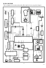
1. POWER SUPPLY
The power supply circuit of the EB4-A chassis is
composed of a rectifier smoothing circuit, an oscillation
circuit, a control circuit and an output rectifier circuit. The
AC input voltage is full-wave rectified by the rectifier
smoothing circuit, and an unstable DC voltage is
generated at both terminals of the smoothing capacitor
C607. This voltage is input to the oscillation circuit. The
oscillation circuit is provided with a blocking oscillator
circuit that switches the switching transistor Q613 ON
and OFF, and an oscillation frequency and a duty square
wave pulse are generated in the input windings
according to operation of the control circuit. A square-
wave pulse whose size is dependent on the turn ratio of
the input and output windings is obtained in the output
winding. This is rectified in the output rectifier circuit, and
the desired DC voltage is obtained.
2. IF & DEFLECTION (TDA8361)
The IF output signal from the tuner passes through the
SAW filter, and it is input to pin45 and pin46 of IC201.
The signal input to the IC passes through the IF
amplifier, video detection and video amplifier circuits and
is output from pin7 as a composite video signal. And
after this signal is converted to impedance at Q151,
supplies to the video and chroma amplifier stages.
The sync.-separation circuit separates the video signals
applied to pin13(internal video signal) or pin15(external
video signal) to vertical- and horizontal-sync. signals
respectively. The horizontal oscillator requires no
external components and is fully integrated. The
oscillator is always running when the start-pin36 is
supplied with 8V. Horizontal drive signal is output from
pin37. VR361 is for adjustment of the horizontal centring.
The separated vertical-sync. signal from sync. separation
circuit passes through the vertical-separation circuit, and
applied to trigger divider circuit. The horizontal oscillation
pulse and input vertical sync. pulse are monitored by the
trigger divider circuit, and switching 50Hz and 60Hz
system, the vertical amplitude automatically adjusted for
50Hz and 60Hz. The output signal from the trigger
divider is triggered vertical oscillation circuit consisting of
C351, R352 and pin42, and vertical drive pulse is output
from pin43. VR501 is for changing the amount of AC
feedback applied to pin41 and for adjustment of the
vertical amplitude.
3. VIDEO CHROMA & R.G.B. (TDA8361)
The composite video signal output from the pin7 of
IC101 passes through Q151-Q154, and it is supplied to
pin13. The external video signal output from SCART is
supplied to pin15. The video signal input to pin13 or
pin15 is separated to luminance (Y) signal and chroma
signal in IC201. These pins are used in common with
H/V-sync. separation input. The peaking of Y signal is
adjusted by DC voltage of pin14. (“SHARPNESS”
control) The chroma signal is divided into R-Y and B-Y
chroma signals, demodulated in IC201, and output from
pin30 (R-Y) and pin31 (B-Y). These chroma signals pass
through the 1H delay line circuit (IC271), and they are
input to pin29 (R-Y) and pin28 (B-Y). These R-Y/B-Y
signals pass through RGB matrix circuit and RGB
selector circuit of IC101. The internal RGB signals are
generated in RGB matrix circuit and the RGB selector,
consisting linear amplifiers, clamps and selects either the
internal RGB signals or the external RGB signals input
from pin22(R), pin23(G), pin24(B). Selection is controlled
by the voltage at the RGB switch control (pin21) and
mixed RGB modes are possible since RGB switching is
fast. The RGB switch also functions as a fast blanking
pin by blanking the RGB output stages; here internal and
external RGB signals are overruled. The colour gain is
controlled by DC voltage of pin26. (“COLOUR” control)
The contrast control voltage present at pin25, and the
brightness control voltage present at pin17 controls DC
level of RGB signals. The RGB signals are finally
buffered before being available at the RGB output pins
[pin20 (R), pin19 (G), pin18 (R)].
4. AUDIO OUTPUT(TDA7263M)
The audio signals output from the audio unit are input to
pin1(L) and 5(R) of IC171 and passes through the pre-
amplifier circuit and drive circuit, after which it is input to
the audio amplifier. The audio amplifier is an SEPP
(single-ended, push-pull) OTL type and output to pin8(R)
and 10(L) to directly drive the speakers.
5. VERTICAL OUTPUT (LA7832/LA7832)
An IC (LA7832/LA7833) is used for the vertical output
circuit in this chassis. The vertical drive pulse from pin43
of IC201 is input to pin4 of IC501. This pulse drives
IC501, and vertical scanning is performed. In the first half
of scanning a deflecting current is output from pin2 and
passes through the following path:
Vcc(B4)
➞
D501
➞
pin3
➞
pin2
➞
DY
➞
C512
➞
VR501/R509. An electric charge is then stored in C512.
In the last half of scanning the current path is C512
➞
DY
➞
pin2
➞
pin1
➞
VR501/R509
➞
C512. In this way,
an amplifying sawtooth waveform current flows directly to
DY to perform electron beam defection. Next, in the first
half of the banking period the vertical drive pulse
suddenly becomes OFF, and in order to reduce the
current flowing to DY, the current path becomes as
follows by the inductance of DY:
DY
➞
pin2
➞
pin1
➞
VR501/R509
➞
C512
➞
DY. Also,
when the charge of DY has dissipated, the current path
becomes Vcc24V
➞
pin6
➞
pin7
➞
C502
➞
pin3
➞
pin2
➞
DY
➞
C512
➞
VR501/R509, and when the
prescribed current value is reached, the vertical drive
pulse becomes ON. This completes one cycle.
CIRCUIT DESCRIPTION


