7-2
Samsung Electronics
Schematic Diagram
This Document can not be used without Samsung’s authorization.
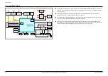
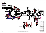
7-1 Overall Block Diagram
VCC_2.8
Nand Flash
SDRAM
SD256M16E
32MB(16M*16)
TFT LCD(262K color)
TS-180T-008A
(176*220)
LCD_D[0..15]
Processor
(S5L8700)
- 32bit ARM940T(200Mhz)
- 16bit CalmADM2E(120Mhz)
- 256kb SRAM
I2S
I2S
ADC
NF_D[0-7]
XD[0-15]
XA[1-12]
USB
Power On
USB 5V
VCC_2.8
VCC_2.8
VDD_BATT
SPK_VDD 5V
VCC_2.8
USB 5V
Core_1.2
VCC_2.8
VCC_2.8
VCC_2.8
Line In
Line Out
SPK_VDD
CORE_1.2
VCC_2.8
VCC_BATT
USB
Jack
Charge Pump
(AAT3151)
HALL IC
(HED52XXU11)
Amp
MAX1760
Li-Polymer
Batt.
600mAh
Bluetooth
(LBMA465CP3)
CODEC
(WM1800G)
Earphone
Speaker
MIC
DC/DC
Converter
Charger IC
(AAT2550)
Reset
DFU
32.768KHz
/12Mhz
RTC
S-35392A
FM Tuner
(Si4702)
ECHO
(FM2010)
Touch
Key PAD
UART
Line-In
Line-Out
USB
Controller
I2S
Uart RX, TX
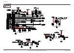
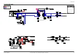
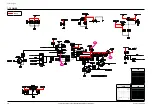
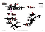
The Main System contains basic circuit blocks, such as Processor (S5L8700), SDRAM, Flash Memory, Power Block,
Audio DAC, etc., and function blocks, such as FM-Tuner, Bluetooth Block, Hal IC, and etc. The display is connected to
a 1.8-inch TFT LCD.
Serial Interfaces between ICs are implemented with various Protocols throughout the System. A host processor
(S5L8700) UART is used to implement CODEC and FM Tuner features.
The interface between the Bluetooth Module and the Host Processor is achieved through UART, and the audio DAC
achieves mode setting and data transfer through I2C and I2S, respectively.
Power can be turned On and Off with the Power S/W located at the top of the set. Either the built-in battery or the
power adapter can be used for power supply. The power adapter is capable of 5V input. Power from the power adapter
is used to recharge the battery at AAT2550 and generates power for the system (2.8V, 1.2V).


