


Samsung Electronics
1-3
1-3 Precautions for Electrostatically Sensitive Devices (ESDs)
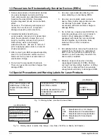
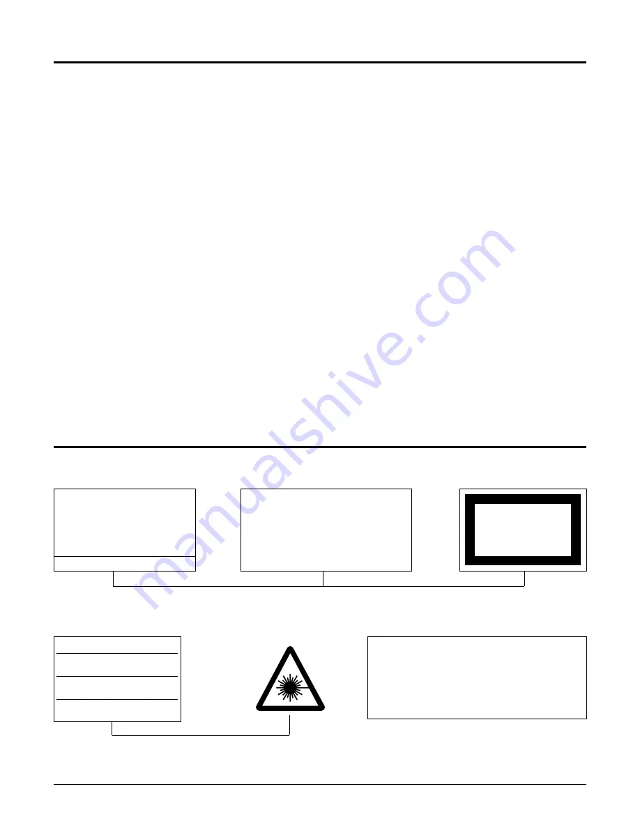
1-4 Special Precautions and Warning Labels for Laser Products
1. Some semiconductor ("solid state") devices
are easily damaged by static electricity.
Such components are called Electrostatically
Sensitive Devices (ESDs). Examples
include integrated circuits and some field-
effect
transistors. The following techniques will
reduce the occurrence of component
damage caused by static electricity.
2. Immediately before handling any
semiconductor components or assemblies,
drain the electrostatic charge from your
body by touching a known earth ground.
Alternatively, wear a discharging
wrist-strap device. (Be sure to remove it
prior to applying power--this is an electric
shock precaution.)
3. After removing an ESD-equipped assembly,
place it on a conductive surface such as
aluminum foil to prevent accumulation of
electrostatic charge.
4. Do not use freon-propelled chemicals.
These can generate electrical charges that
damage ESDs.
5. Use only a grounded-tip soldering iron
when soldering or unsoldering ESDs.
6. Use only an anti-static solder removal
device. Many solder removal devices are
not rated as "anti-static" (these can
accumulate sufficient electrical charge to
damage ESDs).
7. Do not remove a replacement ESD from its
protective package until you are ready to
install it. Most replacement ESDs are
packaged with leads that are electrically
shorted together by conductive foam,
aluminum foil or other conductive
materials.
8. Immediately before removing the protective
material from the leads of a replacement
ESD, touch the protective material to the
chassis or circuit assembly into which the
device will be installed.
9. Minimize body motions when handing
unpackaged replacement ESDs. Motions
such as brushing clothes together, or lifting
a foot from a carpeted floor can generate
enough static electricity to damage an ESD.
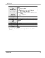
Precautions
UL
: Manufactured for U.S.A. Market.
CSA
: Manufactured for Canadian Market.
EU
: Manufactured for European Market.
SCAN : Manufactured for Scandinavian
Market.
This Product Complies with
DHHS Rules 21CFR, Sub
chapter J.At date of Manu-
facture
(UL)
(UL,CSA,SCAN)
(EU)
CERTIFIED ONLY TO CANADIAN
ELECTRICAL CODE.
CERTIFIE EN VERTU DU CODE
CANADIAN DE LELETRICITE
SEULEMENT
(CSA)
CLASS 1
LASER PRODUCT
(UL,CSA,EU)
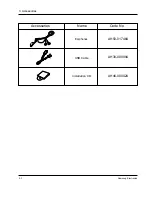
Fig. 1-3 Warning Labels (Location: Enclosure Block)
Fig. 1-4 Warning Labels (Location: Disc Clamper, Inner Side of Unit Door or Nearby Unit Chassis )
CAUTION :
INVISIBLE LASER RADIATION WHEN OPEN
AND INTERLOCKS DEFEATEO AVOIDEXPOSURE TO BEAM
ADVARSEL:
USYNLIG LASERSTRÅLING VED ABNING
NÅR SIKKERHEDSAFBRYDERE ER UDE AF FUNKTION
UNDGA UDSAETTELSE FOR STRALING
VARO:
AVATTAESSA JA SUOJALUKITUS OHITETTAESSA
OLET ALTTINA NAKYMATTÖMALLE LASERSATEILYLLE ALA
KATSO SATEESEEN!
VARNING:
OSYNLIG LASERSTRÅLNING NAR DENNA DEL
AR OPPNAD OCH SPARREN AR URKOPPLAD BETRAKTA
EJSTRÅLEN!
Summary of Contents for yePP YP-K5JAB
Page 2: ...ELECTRONICS Samsung Electronics Co Ltd AUG 2006 Printed in Korea Code no AH68 01819S ...
Page 19: ...Samsung Electronics 4 1 Samsung Electronics 4 Adjustments 1 How to recover the device ...
Page 20: ...4 2 Samsung Electronics ...
Page 21: ...4 3 Samsung Electronics ...
Page 22: ...4 4 Samsung Electronics ...
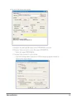
Page 23: ...4 5 Samsung Electronics 2 How to upgrade Firmware ...
Page 24: ...4 6 Samsung Electronics ...
Page 25: ...4 7 Samsung Electronics ...
Page 26: ...4 8 Samsung Electronics ...
Page 27: ...4 9 Samsung Electronics ...
Page 28: ...4 10 Samsung Electronics ...
Page 29: ...4 11 Samsung Electronics ...
Page 34: ...6 Troubleshooting 1 Power failure Samsung Electronics 6 1 ...
Page 35: ...2 When you cannot hear through the earphones 6 2 Samsung Electronics ...
Page 36: ...3 When you cannot hear through the built in speaker Samsung Electronics 6 3 ...
Page 37: ...6 4 Samsung Electronics 4 When the Touch Pad does not work properly ...
Page 38: ...6 5 Samsung Electronics 5 When you cannot connect the player to the PC ...
Page 42: ...9 1 Samsung Electronics 9 BLOCK DIAGRAM 9 BLOCK DIAGRAM ...
Page 43: ...Samsung Electronics 10 1 10 Wiring Diagram ...
Page 44: ...10 2 Samsung Electronics ...
Page 45: ...10 3 Samsung Electronics ...
Page 46: ...10 4 Samsung Electronics ...
Page 47: ...Samsung Electronics 11 1 11 PCB Diagram ...
Page 49: ...Samsung Electronics 12 2 2 MEMORY ...
Page 50: ...12 3 Samsung Electronics 3 LCD ...
Page 51: ...Samsung Electronics 12 4 4 USB ...
Page 52: ...12 5 Samsung Electronics 5 AUDIO CODE ...
Page 53: ...Samsung Electronics 12 6 6 POWER ...
Page 54: ...12 7 Samsung Electronics 7 FM ...
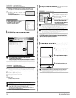
Page 56: ...Samsung Electronics 12 9 When you touch the Touch Pad ...
Page 58: ...Samsung Electronics 12 11 Open Landscape View Close Portrait View ...
Page 59: ...12 12 Samsung Electronics ...
Page 60: ...Samsung Electronics 13 1 13 Circuit Board Description 1 CPU Block 2 SDRAM 3 NAND Flash ...
Page 61: ...13 2 Samsung Electronics 9 PBA Port ...
Page 62: ...Samsung Electronics 13 3 ...
Page 63: ...13 4 Samsung Electronics ...
Page 66: ...14 2 Samsung Electronics Yepp Block Diagram ...
Page 74: ...14 10 Samsung Electronics Small Form factor Cards Comparison ...