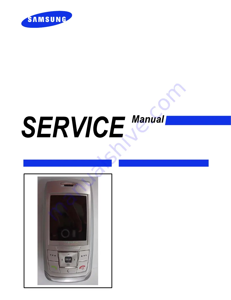
background image

GSM TELEPHONE

SGH-E250

GSM TELEPHONE

CONTENTS

1.

Safety Precautions

2.

Specification

3.

Product Function

4.

Array course control

5.

Exploded View/Disassembly

and Assembly Instructions

6.

MAIN Electrical Parts List

7.

Block Diagrams

8.

PCB Diagrams

9.

Flow Chart of Troubleshooting

10.

Reference data

Summary of Contents for SGH

Page 1: ...S 1 Safety Precautions 2 Specification 3 Product Function 4 Array course control 5 Exploded View Disassembly and Assembly Instructions 6 MAIN Electrical Parts List 7 Block Diagrams 8 PCB Diagrams 9 Flow Chart of Troubleshooting 10 Reference data ...

Page 2: ...ss 2 2 3 Product Function 4 Array course control 4 1 Sofrware Adjustments 4 1 4 2 Sofrware Downloading 4 2 5 Exploded View Disassembly Assembly Instructions 5 1 Cellular phone Exploded View 5 1 5 2 Cellular phone Parts list 5 2 5 3 Disassembly Assembly Instructions 5 4 6 MAIN Electrical Parts List 7 Block Diagrams 7 1 Base Band Block Diagram 7 1 7 2 RF Block Diagram 7 2 8 PCB Diagrams ...

Page 3: ...Melody 9 11 9 7 Key Data Input 9 13 9 8 Receiver Part 9 14 9 9 Back Light for Color Main LCD 9 15 9 10 Key Back Light 9 17 9 11 Camera Part 9 19 9 12 GSM Receiver 9 21 9 13 GSM Transmitter 9 22 9 14 DCS Receiver 9 23 9 15 DCS Transmitter 9 24 9 16 PCS Receiver 9 25 9 17 PCS Transmitter 9 26 9 18 Bluetooth Part 9 28 9 19 Radio Part 9 30 10 Reference data ...

Page 4: ...worn away Use a thicken twisted wire when you measure level A thicken twisted wire has low resistance therefore error of measurement is few Repair after separate Test Pack and Set because for short danger for example an overcurrent and furious flames of parts etc when you repair board in condition of connecting Test Pack and tuning on Take specially care of soldering because Land of PCB is small a...

Page 5: ...ined your body before you touch semiconductor or parts with semiconductor There are ways that you touch an earthed place or wear static electricity prevention string on wrist Use earthed soldering steel when you connect or disconnect ESD Use soldering removing tool to break static electricity otherwise ESD will be damaged by static electricity Don t unpack until you set up ESD on product Because m...

Page 6: ...spacing 45MHz 45MHz 95MHz 80MHz Mod Bit rate Bit Period 270 833kbps 3 692us 270 833kbps 3 692us 270 833kbps 3 692us 270 833kbps 3 692us Time Slot Period Frame Period 576 9us 4 615ms 576 9us 4 615ms 576 9us 4 615ms 576 9us 4 615ms Modulation 0 3GMSK 0 3GMSK 0 3GMSK 0 3GMSK MS Power 33dBm 5dBm 33dBm 5dBm 30dBm 0dBm 30dBm 0dBm Power Class 5pcl 19pcl 5pcl 19pcl 0pcl 15pcl 0pcl 15pcl Sensitivity 102dBm...

Page 7: ... control level DCS1800 0 30 3 dBm 1 28 3 dBm 2 26 3 dBm 3 24 3 dBm 4 22 3 dBm 5 20 3 dBm 6 18 3 dBm 7 16 3 dBm 8 14 3 dBm 9 12 4 dBm 10 10 4 dBm 11 8 4dBm 12 6 4 dBm 13 4 4 dBm 14 2 5 dBm 15 0 5 dBm TX Power control level PCS1800 0 30 3 dBm 1 28 3 dBm 2 26 3 dBm 3 24 3 dBm 4 22 3 dBm 5 20 3 dBm 6 18 3 dBm 7 16 3 dBm 8 14 3 dBm 9 12 4 dBm 10 10 4 dBm 11 8 4dBm 12 6 4 dBm 13 4 4 dBm 14 2 5 dBm 15 0 ...

Page 8: ...ization Main Function SlimSlide Design Intenna VGA Camera Bluetooth V 2 0 Stereo Bluetooth Headset Mobile Tracker SOS Messaging Large 2 0 65K Color TFT Display SMS MMS E Mail WAP 2 0 Java MIDP 2 0 MP3 AAC MP4 3GPP Decoding Video Recording and Messaging GSM GPRS Class 10 Triple Band GSM900 DCS PCS 64 Poly Speaker Phone Voice Clarity ...

Page 9: ...SAMSUNG Proprietary Contents may change without notice Product Function 3 2 This Document can not be used without Samsung s authorization ...

Page 10: ... may change without notice 4 Array course control 4 1 This Document can not be used without Samsung s authorization 4 1 Software Adjustments Power Supply Cable Serial Cable CSA LL64151 A Test Jig GH80 03306A Test Cable GH39 00499A ...

Page 11: ...loder V1 2 Lite For PNX5230 exe E250 Mobile Phone Data Cable Binary file TFS file 4 2 2 S W Downloader Program Load the binary download program by executing the OneNAND Downloder V1 2 Lite For PNX5230 exe 1 Select the connected serial port and the rate of speed 2 Select the check box the mode you want to download if the binary file wanted check only BIN if the tfs file wanted check only TFS if all...

Page 12: ...SAMSUNG Proprietary Contents may change without notice Array course control 4 3 This Document can not be used without Samsung s authorization 3 Select the file s what you want to download ...

Page 13: ...SAMSUNG Proprietary Contents may change without notice Array course control 4 4 This Document can not be used without Samsung s authorization ...

Page 14: ... authorization 5 Exploded View Disassembly Assembly Instructions 5 1 Cellular phone Exploded View QFU01 QKP02 QKP01 QMW01 QME03 QME02 QFR01 QCW01 QCA05 QCR17 QSC05 QSC06 QSP01 QMO01 QLC01 QCA01 QSD01 QHI01 QIF01 QFL01 QME01 QBR03 QMI03 QMI01 QAN02 QMP01 QRE01 QSC13 QRF01 QBA00 QCR03 QBA01 QVO01 QCR03 QMP02 ...

Page 15: ...AIN EU SIL GH98 02264A QKP02 ASSY KEYPAD SUB EU SIL GH98 02263A QME01 UNIT KEY FPCB GH59 03615A QME03 MEA SLIDE FPCBKIT GH97 06873A QMI01 MICROPHONE ASSY GH30 00309A QMI03 RMO RUBBER MIC GH73 08308A QMP01 PBA MAIN SGH E250 MAIN GH92 03188A QRE01 ASSY CASE REAR GH98 02262A QRF01 MPR TAPE RF SHEET GH74 27453A QSC05 RMO RUBBER SCREW SLIDE L GH73 08309A QSC06 RMO RUBBER SCREW SLIDE R GH73 08310A QSC13...

Page 16: ...ER SOAK GH68 02026A LABEL P WATER SOAK GH68 02026A MANUAL USERS XEG GERMAN GH68 12415A LABEL R MAIN EU GH68 12733A BOX UNIT EU GH69 04558A CUSHION CASE EU GH69 04565A RMO RUBBER SIM GH73 08686A MPR BOHO VINYL MAIN WIN GH74 16880A MPR INSU TAPE GH74 27455A MPR INSU TAPE GH74 27456A MPR ELEC TAPE GH74 27457A MPR ELEC TAPE GH74 27495A MPR TAPE LABEL GH74 28874A MPR INSU TAPE GH74 29298A MPR SPONGE GH...

Page 17: ...nsforming the rear cover 1 Be careful of body damage and scretch 1 Be careful of damaging F PCB 1 Be careful of damaging components 1 Remove the RF Sheet SCREW Cover of rear 2 Unscrew 5 screws 1 1 Remove the volumn Key 2 Disassemble the connector 2 3 1 Open the T Flash power cover 2 Lift main board 3 Detach the LCD Connector after slide down 4 1 Separate board from the set 5 3 Disassembly and Asse...

Page 18: ...be used without Samsung s authorization 1 Be careful of damaging FPCB detaching Volumn Key Fpcb 2 Be careful of body damage and scretch 1 Be careful of body damage and scretch 5 6 7 8 1 Remove the EMI tape 1 Detach the Volumn Key Fpcb 2 Disassemble key can from the point of the picture 1 Disassemble the key pad 1 Unscrew 2 screws ...

Page 19: ... Be careful of damaging F PCB 1 Be careful of body damage and scretch 2 Be careful of damaging camera F PCB 9 10 11 12 1 Unscrew 4 screws 2 Disassemble the upper with a couple of thumbs pressing the point of picture 1 Match the hole of LOWER and FRONT holding up the slide 2 Draw out the FPCB from the hole 1 Remove the tape covering FPCB Connector 2 Disassemble FPCB after lifting Connector 1 Disass...

Page 20: ...ions 5 7 This Document can not be used without Samsung s authorization 1 Be careful of body damage and scretch 2 Be careful of sticking between two sides tape and LCD 13 1 Disassemble from upper after lifting lightly the upside of the Sub PBA 2 Disassemble SPK MOT CAMERA 1 Disassemble Sub Key Pad 15 ...

Page 21: ...g CAMERA FPCB 1 Be careful of body damage and scretch 2 Be careful of damaging F PCB 1 Be careful of damaging F PCB 1 2 3 4 1 Joint the Sub Key Pad 1 Assemble Sub PBA inserting the bottom of the board 2 Assemble CAMERA SPK MOT after inserting camera FPCB 1 Insert FPCB CON TO CON 2 Attach conserving TAPE 1 Match the hole pulling down lightly the SLIDE ASSY like picture 2 Insert FPCB Assembly ...

Page 22: ...ung s authorization 1 Be careful of body damage and scretch 1 Be careful of body damage and scretch 1 Be careful of body damage and scretch 1 Check up the fitting between key pad and REAR 7 8 1 Insert both screw caps in each direction 1 Assemble the key pad in FRONT 7 8 1 Assemble SLIDE ASSY part 2 Assemble from the bottom side 1 Screw down 4 screws ...

Page 23: ...n 1 Be careful of damaging F PCB 1 Check up whether tape color is same with SET color or not 1 Be careful of damaging BGA components 1 Be careful of body damage and scretch 10 9 1 Attach the EMI tape 1 Assemble the key can 2 Check up the attaching FPCB in Volumn Key side 11 12 1 Assemble the FPCB with main board 1 Open the T Flash Power Cover 2 Assemble the main board ...

Page 24: ...sembly Instructions 5 11 This Document can not be used without Samsung s authorization 1 Be careful of damaging BGA components 1 Be careful of body damage and scretch 13 1 Insert the Volumn Key 2 Assemble the Key Connector 1 Screw down 5screws 2 Attach RF Sheet SCREW Cover of rear 14 ...

Page 25: ...SAMSUNG Proprietary Contents may change without notice Exploded View Disassembly Assembly Instructions 5 12 This Document can not be used without Samsung s authorization ...

Page 26: ...A C123 C CER CHIP 2203 005061 SA C125 C CER CHIP 2203 001221 SA C126 C CER CHIP 2203 005061 SA C128 C CER CHIP 2203 000233 SA C131 C CER CHIP 2203 000233 SA C201 C CER CHIP 2203 005482 SA C202 C CER CHIP 2203 000812 SA C203 C CER CHIP 2203 005482 SA C204 C CER CHIP 2203 005482 SA C205 C CER CHIP 2203 005482 SA C206 C CER CHIP 2203 005482 SA C208 C CER CHIP 2203 005482 SA C209 C CER CHIP 2203 00548...

Page 27: ...CER CHIP 2203 005736 SA C413 C CER CHIP 2203 006257 SA C414 C CER CHIP 2203 006562 SA C415 C CER CHIP 2203 006562 SA C416 C CER CHIP 2203 000550 SA C417 C CER CHIP 2203 000550 SA C420 C CER CHIP 2203 006257 SA C421 C CER CHIP 2203 006324 SA C422 C CER CHIP 2203 006423 SA C423 C CER CHIP 2203 006562 SA C424 C CER CHIP 2203 006562 SA C425 C CER CHIP 2203 006361 SA C426 C CER CHIP 2203 006361 SA C427...

Page 28: ...P 2203 001259 SA C549 C CER CHIP 2203 005050 SA C550 C CER CHIP 2203 005393 SA C551 C CER CHIP 2203 000278 SA C601 C CER CHIP 2203 006423 SA C602 C CER CHIP 2203 005061 SA C603 C CER CHIP 2203 006423 SA C604 C CER CHIP 2203 000812 SA C605 C CER CHIP 2203 000425 SA C606 C CER CHIP 2203 006562 SA C607 C CER CHIP 2203 006562 SA C609 C CER CHIP 2203 006562 SA C610 C CER CHIP 2203 006562 SA C611 C CER ...

Page 29: ...339 SA Q600 FET SILICON 0505 001518 SA R101 R CHIP 2007 001313 SA R103 R CHIP 2007 000140 SA R201 R CHIP 2007 000143 SA R202 R CHIP 2007 000171 SA R204 R CHIP 2007 000171 SA R205 R CHIP 2007 000148 SA R206 R CHIP 2007 002796 SA R209 R CHIP 2007 000140 SA R212 R CHIP 2007 000170 SA R213 R CHIP 2007 000148 SA R214 R CHIP 2007 000170 SA R215 R CHIP 2007 001319 SA R217 R CHIP 2007 001319 SA R218 R CHI...

Page 30: ...1333 SA R505 R CHIP 2007 007142 SA R506 R CHIP 2007 000172 SA R507 R CHIP 2007 002796 SA R508 R CHIP 2007 002796 SA R509 R CHIP 2007 000172 SA R510 R CHIP 2007 000171 SA R516 R CHIP 2007 007528 SA R518 R CHIP 2007 007528 SA R519 R CHIP 2007 007528 SA R523 R CHIP 2007 000162 SA R524 R CHIP 2007 003001 SA R525 R CHIP 2007 000148 SA R526 R CHIP 2007 008055 SA R529 R CHIP 2007 001333 SA R601 R CHIP 20...

Page 31: ...202 FILTER EMI SMD 2901 001316 SA U300 IC ASIC SGHE420 GH13 00042A SA U301 IC CMOS LOGIC 0801 002237 SA U302 IC CMOS LOGIC 0801 002237 SA U402 IC POSI FIXED REG 1203 003737 SA U403 IC POWER SUPERVISOR 1203 004382 SA U404 IC POSI FIXED REG 1203 003737 SA U500 IC AUDIO AMP 1201 002492 SA U501 IC DEMODULATOR 1204 002688 SA U503 IC ANALOG SWITCH 1001 001231 SA U504 IC ANALOG SWITCH 1001 001231 SA U601...

Page 32: ...SAMSUNG Proprietary Contents may change without notice This Document can not be used without Samsung s authorization 7 Block Diagrams 7 1 7 1 Base Band Block Diagram ...

Page 33: ...SAMSUNG Proprietary Contents may change without notice Block Diagrams 7 2 This Document can not be used without Samsung s authorization 7 2 RF Block Diagram ...

Page 34: ...SAMSUNG Proprietary Contents may change without notice 8 PCB Diagrams 8 1 This Document can not be used without Samsung s authorization Top ...

Page 35: ...SAMSUNG Proprietary Contents may change without notice PCB Diagrams 8 2 This Document can not be used without Samsung s authorization Bottom ...

Page 36: ...ower On does not work Change the Battery END No Yes C420 VISA 2 7V Check the PMU related to VINT No Yes Check the Clock at R410 32KHZ Resolder OSC400 No Yes C400 VDD_IO_LOW C405 VDD_IO_HIGH H Check the related circuit No Yes C205 VDD_GSM_CORE 1 8V Check the VDD_GSM_CORE circuit No Yes Check for the clock at C325 26MHz Check the clock generation circuit related to U102 No Yes Check the initial oper...

Page 37: ...SAMSUNG Proprietary Contents may change without notice This Document can not be used without Samsung s authorization Flow Chart of Troubleshooting 9 2 ...

Page 38: ...ubleshooting This Document can not be used without Samsung s authorization 9 3 9 2 Initial UCP200 pin C11 RSTON H Initial Failure Check the circuit related to reset END No Yes UCP200 pin F1 R221 RSTEXTn H OK Yes Yes No change UCP200 Check the 16bit data signal memory CE Yes ...

Page 39: ...SAMSUNG Proprietary Contents may change without notice This Document can not be used without Samsung s authorization Flow Chart of Troubleshooting 9 4 ...

Page 40: ... not be used without Samsung s authorization 9 5 9 3 Charging Part Check the U403 pin 38 4 9V Abnormal charging part END No Yes U403 pin 34 AUX_ON L No Yes Check the U403 pin 46 1 4V No Yes Check the circuit related to V_EXT_CHARGE Check the circuit related to AUX_ON signal Resolder or replace U403 Yes ...

Page 41: ...SAMSUNG Proprietary Contents may change without notice This Document can not be used without Samsung s authorization Flow Chart of Troubleshooting 9 6 ...

Page 42: ...d without Samsung s authorization 9 7 9 4 Sim Part SIM400 pin 1 5 H Phone can t access SIM Card Resolder or replace U403 Check the SIM Card END No Yes Yes Yes No Check the Clock After Power ON Check SIMCLK Signal on pin3 of SIM400 in a few second Yes No Replace PBA After SIM card insert SIM400 pin 2 H SIM_RST Yes ...

Page 43: ...SAMSUNG Proprietary Contents may change without notice This Document can not be used without Samsung s authorization Flow Chart of Troubleshooting 9 8 ...

Page 44: ...e used without Samsung s authorization 9 9 9 5 Microphone Part Check the connection from MIC Check the circuit from UCP200 to MIC Resolder MIC Resolder the C514 C520 R516 R519 END No Yes Yes Yes Yes No Check F500 PIN 8 H No Check the JACK_IN signal Microphone does not work Yes Check the MIC No Replace the MIC ...

Page 45: ...SAMSUNG Proprietary Contents may change without notice This Document can not be used without Samsung s authorization Flow Chart of Troubleshooting 9 10 ...

Page 46: ...e used without Samsung s authorization 9 11 9 6 Speaker Part Melody U500 pin 7 2 9V Speaker does not work U500 pin 15 17 1 8V When U500 operate Resolder U500 No Yes No Resolder or replace U500 Yes HDC600 pin 2 3 1 8V When U500 operate Resolder HDC600 No Yes END Yes Is Speaker working Change the Speaker No Yes ...

Page 47: ...SAMSUNG Proprietary Contents may change without notice This Document can not be used without Samsung s authorization Flow Chart of Troubleshooting 9 12 ...

Page 48: ...ing This Document can not be used without Samsung s authorization 9 13 9 7 Key Data Input When one of the keys is pushed is it displayed on LCD Check the Dome sheet Key Pad END No Yes Yes Check Initial Operation When one of the keys is pushed KBIO signal is OK Replace the PBA No Yes ...

Page 49: ...ce This Document can not be used without Samsung s authorization Flow Chart of Troubleshooting 9 14 9 8 Receiver Part Is Receiver working Resolder UCP200 or Change PBA END No Yes Yes Receiver does not work No Replace the Receiver Yes Is Receiver working ...

Page 50: ...shooting This Document can not be used without Samsung s authorization 9 15 9 9 Back Light for Color Main LCD Is LCD Contrast set on high level in the Menu Set LCD Contrast on high level END No Yes Yes Backlight does not work HDC600 PIN 21 H Resolder HDC600 or change PBA No Yes ...

Page 51: ...SAMSUNG Proprietary Contents may change without notice This Document can not be used without Samsung s authorization Flow Chart of Troubleshooting 9 16 ...

Page 52: ...thout notice Flow Chart of Troubleshooting This Document can not be used without Samsung s authorization 9 17 9 10 Key Back Light U906 pin6 H Check the U906 related to VDD_KEY END No Yes Yes Main Key LED does not work U906 pin3 3 3V Change U906 ...

Page 53: ...SAMSUNG Proprietary Contents may change without notice This Document can not be used without Samsung s authorization Flow Chart of Troubleshooting 9 18 ...

Page 54: ...amsung s authorization 9 19 9 11 Camera part Camera function does not work Yes No Reconnect the camera module Check the Camera connector on LCD module Yes HDC600 Pin21 H No Resolder HDC600 or change PBA Yes C310 26MHz No Check U102 pin8 related to 26MHz and C131 Yes Is there another problem END Replace the camera module Yes ...

Page 55: ...SAMSUNG Proprietary Contents may change without notice This Document can not be used without Samsung s authorization Flow Chart of Troubleshooting 9 20 ...

Page 56: ...circuit Resolder F100 Check Resolder C117 L123 C126 And PMU Part Resolder U102 RX ON RF input CH center freq 67 7kHz Cell Power 60dBm Yes F100 Pin13 65dBm No Resolder CN205 C103 L102 Yes F100 1 2 68dBm Check F100 pin9 pin11 L No No Yes Yes No Resolder C108 C109 L105 U101 pin 24 70dBm pin 25 70dBm Yes No U101pin 16 17 29 32 36 2 8V pin10 1 8V U101 pin 4 5 6 7 0 2Vp_p No Yes Yes Check UCP200 END ...

Page 57: ...eck UCP200 END No Yes No Yes Yes Yes Yes Yes Yes No Yes No No No No Check U102 C117 C126 L123 Check VBAT or PAM control signal Resolder or Change U103 Check U103pin 2 3 5 6 8 Vbatt pin4 OK Yes U102 pin 4 5 6 7 0 2Vp_p Resolder or Change L101 Check ANT Switch control circuit Change or Resolder F100 U103 pin7 4dBm U103 pin12 30dBm F100 pin10 30dBm Check F100 pin11 H 2 6V Pin9 L TX ON 5Level Resolder...

Page 58: ...k UCP201 No No No No No Yes Yes Yes Yes Yes Yes Resolder U102 Check Resolder U102 C117 C123 C126 And PMU Part U101 pin16 17 29 32 36 2 8V pin 10 1 8V Resolder C104 C105 L104 Resolder F100 Check ANT Switch control circuit U102 pin 22 70dBm pin 23 70dBm U101 pin 4 5 6 7 0 2Vp_p F100 3 4 68dBm RX ON RF input CH center freq 67 7kHz Cell Power 60dBm Yes No END Resolder CN205 C103 L102 F100 Pin13 65dBm ...

Page 59: ...ND No Yes No No No Yes Yes Yes Yes No Yes Yes No No No Check Resolder U102 C117 L123 C126 And PMU Part Check VBAT or PAM control signal Resolder or Change U103 Check U103pin 2 3 5 6 8 Vbatt pin4 OK Yes U101 pin 4 5 6 7 0 2Vp_p Resolder or Change C112 L108 Check ANT Switch control circuit Change or Resolder F100 U103 pin1 4dBm U103 pin18 25dBm F100 pin8 25dBm Check F100 pin9 H 2 6V pin11 L TX ON 0L...

Page 60: ...eq 67 7kHz Cell Power 60dBm Yes F100 Pin13 65dBm No Resolder CN205 C103 L102 Yes F100 5 6 68dBm Check F100 pin9 pin11 L No No Check ANT Switch control circuit Yes Yes Resolder F100 U101 pin 20 70dBm pin 21 70dBm No Resolder C101 C102 L103 Yes U101pin16 17 29 32 36 2 8V pin 10 1 8V U101 pin 4 5 6 7 0 2Vp_p No No Check Resolder U102 C117 L123 C126 And PMU Part Yes Yes Resolder U102 Check UCP201 END ...

Page 61: ...ND No Yes No No No Yes Yes Yes Yes No Yes Yes No No No Check Resolder U102 C117 L123 C126 And PMU Part Check VBAT or PAM control signal Resolder or Change U103 Check U103pin 2 3 5 6 8 Vbatt pin4 OK Yes U101 pin 4 5 6 7 0 2Vp_p Resolder or Change C112 L108 Check ANT Switch control circuit Change or Resolder F100 U103 pin1 4dBm U103 pin18 25dBm F100 pin8 25dBm Check F100 pin9 H 2 6V pin11 L TX ON 0L...

Page 62: ...SAMSUNG Proprietary Contents may change without notice Flow Chart of Troubleshooting This Document can not be used without Samsung s authorization 9 27 ...

Page 63: ...not work C319 C318 position is 1 8V Resolder C318 C319 and check the PMU part No Yes No Resolder or replace L301 L301 ANT900 Yes OSC1001 Pin 3 is 26MHz 1 4Vp_p Resolder OSC1001 C325 C326 R312 No Yes No END R304 U1126 U1125 1 8V C323 1 7V 32kHz Resolder R304 U1126 U1125 C323 check or Replace U1109 Yes Yes C321 C316 C317 is 1 5V Resolder C316 C317 L303 C321 check or Replace U1109 No Yes Check UCP201...

Page 64: ...SAMSUNG Proprietary Contents may change without notice Flow Chart of Troubleshooting This Document can not be used without Samsung s authorization 9 29 ...

Page 65: ...of Troubleshooting 9 30 9 19 Radio part R524 R529 C533 2 8V Radio does not work R523 R525 C531 C532 2 8V Resolder R523 R525 C531 C532 and check U501 No Yes No Resolder R524 R529 C533 and Check PMU part Yes L505 2V check or Replace U501 No Yes END Yes C537 L506 C538 C539 is OK Resolder C537 L506 C538 C539 No Yes Check UCP201 Yes ...

Page 66: ...SAMSUNG Proprietary Contents may change without notice Flow Chart of Troubleshooting This Document can not be used without Samsung s authorization 9 31 ...

Page 67: ...SAMSUNG Proprietary Contents may change without notice This Document can not be used without Samsung s authorization Flow Chart of Troubleshooting 9 32 ...

Page 68: ...K Binary Phase Shift Keying CA Conditional Access CDM Code Division Multiplexing C I Carrier to Interference DMB Digital Multimedia Broadcasting EN European Standard ES Elementary Stream ETSI European Telecommunications Standards Institute MPEG Moving Picture Experts Group PN Pseudo random Noise PS Pilot Symbol QPSK Quadrature Phase Shift Keying RS Reed Solomon SI Service Information TDM Time Divi...

Page 69: ...SAMSUNG Proprietary Contents may change without notice Reference data 10 2 This Document can not be used without Samsung s authorization ...

Page 70: ...msung Electronics Co Ltd 2006 12 Rev 1 0 ⓒ This Service Manual is a property of Samsung Electronics Co Ltd Any unauthorized use of Manual can be punished under applicable International and or domestic law ...

Reviews: