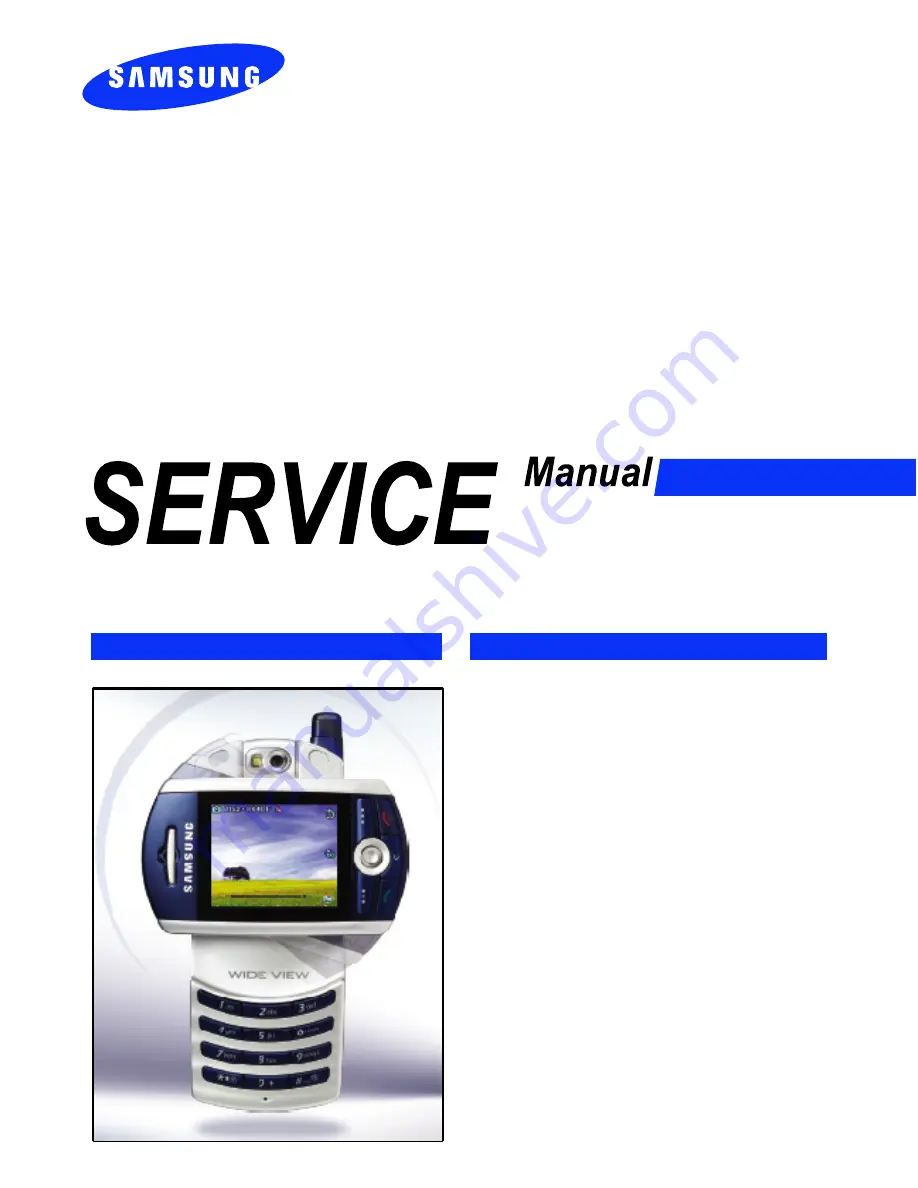
UMTS TELEPHONE
SGH-Z130
CONTENTS
1.
Specification
2.
Flow Chart of Troubleshooting
3.
Exploded Views and Parts List
4.
Electrical Parts List
5.
PCB Diagrams
6.
Block Diagrams
Page 1: ...UMTS TELEPHONE SGH Z130 UMTS TELEPHONE CONTENTS 1 Specification 2 Flow Chart of Troubleshooting 3 Exploded Views and Parts List 4 Electrical Parts List 5 PCB Diagrams 6 Block Diagrams ...
Page 2: ...10 2170 ARFCN range 1 124 0 124 975 1023 512 885 10562 10838 Tx Rx spacing 45MHz 45MHz 95MHz 190MHz Mod Bit rate Bit Period 270 833kbps 3 692us 270 833kbps 3 692us 270 833kbps 3 692us 3 84Mcps s Time Slot Period Frame Period 576 9us 4 615ms 576 9us 4 615ms 576 9us 4 615ms 10ms Modulation 0 3GMSK 0 3GMSK 0 3GMSK UL 2BPSk DL QPSK MS Power 33dBm 13dBm 33dBm 5dBm 30dBm 0dBm MAX 24 1 3 dBm MIN 50dBm Po...
Page 3: ...el EGSM900 5 33 2 dBm 6 31 2 dBm 7 29 2 dBm 8 27 2 dBm 9 25 2 dBm 10 23 2 dBm 11 21 2 dBm 12 19 2 dBm 13 17 2 dBm 14 15 2 dBm 15 13 2 dBm 16 11 3 dBm 17 9 3dBm 18 7 3 dBm 19 5 3 dBm TX Power control level DCS1800 0 30 3 dBm 1 28 3 dBm 2 26 3 dBm 3 24 3 dBm 4 22 3 dBm 5 20 3 dBm 6 18 3 dBm 7 16 3 dBm 8 14 3 dBm 9 12 4 dBm 10 10 4 dBm 11 8 4 dBm 12 6 4 dBm 13 4 4 dBm 14 2 5 dBm 15 0 5 dBm ...
Page 4: ...100mA Check the current consumption Download again Power ON Does not work Check Voltage 3 3V The pin 3 of D500 is high END Charge the Battery Check the U500 Check the path of D500 and U500 Check D500 NO NO NO NO NO YES YES YES YES NO check the OSC801 The pin 3 5 of U500 3 3V Check U500 pin 32 1 37V pin 36 1 8V pin 50 56 2 6V pin 84 2 85V YES U500 Check Pin 53 19 2MHz Vpp 500mV YES Check the initia...
Page 5: ...84 VREG_TCXO 10 VREG_USB 64 VREG_WLAN 14 VSW_5V 12 VREG_5V VREG_MMC 39 56 VREG_MSMA 32 VREG_MSMC 36 VREG_MSME 50 VREG_MSMP 28 VREG_PA 69 VREG_RFRX1 33 35 VDD_MSME 29 VDD_PA VDD_RF 71 VDD_RUIM 41 77 VDD_SPKR 65 VDD_WLAN VIB_DRV_N 25 VDD_ANA 54 83 VDD_MAIN 52 VDD_MSM VDD_MSMC 79 75 SPKR_OUT_P 74 SPKR_BYP SPKR_IN_M 78 76 SPKR_IN_P SPKR_OUT_M 63 REF_BYP 62 REF_GND 61 REF_ISET 21 GP1_DRV_N 23 KPD_DRV_N...
Page 6: ...ung s authorization 2 1 2 System Initial The pin 9 of U500 Low High Initial Failure LCD Display OK Sound operation OK END Check the OSC501 Check the LCD part Check the Audio part YES NO NO NO YES YES YES NO NO YES Check the U500 Check the clock generation circuit related to U500 and OSC801 Check the Sleep X tal signal s at C523 Check the clock signal s at R510 ...
Page 7: ...SB_ID USB_OE_N 40 RUIM_M_RST RUIM_RST 43 SBCK 49 47 SBDT 51 SBST 45 SLEEP_CLK 9 57 PS_HOLD 80 REF_OUT RUIM_CLK 38 RUIM_IO 26 34 RUIM_M_CLK 30 RUIM_M_IO 5 ISNS_M 3 ISNS_P KPDPWR_N 24 MSM_INT_N 59 86 NC 87 NC PON_RESET_N ADC_BYP 70 AMUX_IN1 72 AMUX_IN2 82 AMUX_OUT 7 BAT_FET_N 68 CBL0PWR_N CBL1PWR_N 66 4 CHG_CTL_N 85 GND PM6650 1 BAT501 NEG POS C524 Q504 1 3 2 C521 R513 1 3 2 Q502 C535 R500 V_2 6P R5...
Page 8: ...agrams 2 5 This Document can not be used without Samsung s authorization 3 SIM Part Check the voltage at pin 1 of CN501 2 85V Check the circuit related to CN501 Please insert SIM card Check the CN501 s Connection to SIM card END Check the circuit around U400 and data stored in it YES NO NO YES Resolder CN501 ...
Page 9: ...19 DQ2 L6 DQ20 H3 H4 DQ21 DQ22 E6 F7 DQ23 DQ24 F6 D5 DQ25 DQ26 J5 DQ11 DQ12 H6 H5 DQ13 DQ14 J4 G3 DQ15 DQ16 G4 F4 DQ17 DQ18 E4 DNU A10 R1 DNU DNU R2 R9 DNU DNU R10 DQ0 L4 L5 DQ1 DQ10 J6 ALE C4 BA0 J3 BA1 K2 E3 CKE B4 CLE CLK G8 DNU A2 A9 DNU L2 A2 A3 L3 C2 A4 D2 A5 A6 E1 A7 D3 E2 A8 A9 D4 U400 K4 A0 A1 L1 K3 A10 A11 F2 F1 A12 TP402 C400 TP401 C406 SDRAM_D 26 SDRAM_D 27 SDRAM_D 28 SDRAM_D 29 SDRAM_...
Page 10: ...notice SGH Z130 Flow Chart of Troubleshooting and Circuit Diagrams 2 7 This Document can not be used without Samsung s authorization V_2 85USIM R534 C550 C549 C544 C559 R524 3 3 4 4 5 5 6 6 7 G G 8 9 G G 10 CN501 1 1 22 USIM_CLK USIM_RESET USIM_DATA ...
Page 11: ...rams 2 8 This Document can not be used without Samsung s authorization 2 1 4 Charging Part Check the pin 21 22 of CN206 3 3V Check the TC Abnormal charging operation END YES NO Check the pin 1 of CN203 3 3V Check the path of CN206 and CN203 NO See the indicator of charger is red YES YES Again check the CN206 NO ...
Page 12: ...ization C234 R206 R233 R205 V_2 85TCXO R207 R223 R227 R235 R231 C226 25 26 24 3 4 5 6 7 8 9 16 17 18 19 2 20 21 22 23 1 10 11 12 13 14 15 CN206 R234 2 2 3 3 CN202 1 1 R225 C205 R229 R250 C209 R220 C207 R249 R204 ZD202 2 3 3 CN203 1 1 2 R217 V213 R241 R226 C208 R224 D D RTCK TDO TCK TMS TDI TRST VBAT JTAG_RESET_IN BOOT_SW JIG_ON RFR_1 VF USB_VCC CTS_1 RXD_1 TXD_1 DLC_DETECT ...
Page 13: ...ent can not be used without Samsung s authorization 2 1 5 Microphone Part Micro phone does not work Is the assembled status of Microphone O K YES Reassemble the microphone NO Check the DC bias voltage on Mic path The voltage of R242 is 2 6V 10 NO Check the path around MIC Bias circuit Is microphone OK NO Check U100 END YES YES YES ...
Page 14: ... Chart of Troubleshooting and Circuit Diagrams 2 11 This Document can not be used without Samsung s authorization 8 8 9 9 15 16 16 2 2 3 34 4 5 5 6 6 7 7 CN200 1 1 10 10 11 11 12 12 13 13 14 14 15 R246 C 200 3 3V_LED R242 C225 R214 R247 V201 V_MIC C224 C201 MIC1N MIC1P ...
Page 15: ...n 2 1 6 Speaker Part There is no sound from speaker Check the wave of the pin of U301 s clock 19 2MHz NO Check OSC801 and U802 The pin 32 of U301 2 6V The pin 15 of U301 3 3V NO Check the U500 YES YES Are there any signal at the pin 4 of U301 YES Are there any signal at the pin 1 2 of CN502 YES END Check the U301 Check the U302 Replace the speaker NO NO NO YES Is speaker working ...
Page 16: ..._2 6P R306 4 RST WR 28 15 16 SPVSS VDD 7 VREF 9 8 VSS 29 CS IRQ 3 31 RD 11 32 IOVDD 2 LED MTR 19 NC 56 PLLC SPOUT1 17 18 SPOUT2 SPVDD 12 EQ1 EQ2 13 14 EQ3 33 G G 34 G 35 G 36 10 HPOUT L MONO HPOUT R 27 D0 D1 26 25 D2 24 D3 D4 23 D5 22 D6 21 20 D7 U301 A0 30 CLKI 1 C305 C303 C319 C320 NAND_WE YMU_A0 NAND_RE NAND_D 7 NAND_D 6 NAND_D 5 NAND_D 4 NAND_D 3 NAND_D 2 YMU_RST_N YMU_IRQ YMU_CLK YMU_CS_N NAN...
Page 17: ...amsung s authorization 2 1 7 Receiver Part Is the terminal of receiver is ok NO Replace the receiver Are there any signal at the R172 R173 NO Check the U100 and speaker related circuit There is no sound from receiver YES YES Are there any signal at the pin 22 24 of CN207 YES Is receiver working YES END Check the CN207 and soldering Replace the receiver NO NO ...
Page 18: ...15 6 6 7 7 8 8 9 9 39 39 4 4 40 40 41 41 42 42 43 43 44 44 5 5 31 31 32 32 33 33 34 34 35 35 36 36 37 37 38 38 24 24 25 25 26 26 27 27 28 28 29 29 3 3 30 30 17 17 18 18 19 19 2 2 20 20 21 21 22 22 23 23 1 1 10 10 11 11 12 12 13 13 14 14 15 15 16 16 CN207 NAND_WE LCD_RS1 LCD_CS LCD_RESET BACK_LIGHT_EN SCAN_0 SCAN_2 SCAN_3 KEY_3 VOICE_OUT_N VOICE_OUT_P KEY_0 ON_SW SCAN_1 BL_DIM KEY_1 MICOUTN AA19 MI...
Page 19: ...This Document can not be used without Samsung s authorization 2 1 8 Camera Part Camera function does not work Check the connect CN300 NO Connect the CN300 Pin 2 3 of U504 is high NO Check U504 Pin 9 1 8V Pin 10 2 5V NO Pin 7 of CN300 is 24MHz NO END YES YES YES Check the U100 CON800 Resolder or Change Check the U100 YES ...
Page 20: ... 23 24 24 3 3 4 4 12 12 13 13 14 14 15 15 16 16 17 17 18 18 19 19 2 CN300 11 10 10 11 11 C347 R300 V_1 8CAM V305 C348 C350 V_2 5CAM 8 10 IN 1 IN 2 3 IN IN 4 OUT 5 6 OUT 7 OUT OUT F303 9 G G C349 IN 3 4 IN 5 OUT OUT 6 OUT 7 8 OUT F301 G 9 10 G 1 IN 2 IN V_2 5CAM V_1 8CAM FLASH CAM_EN2 CAM_RESET_N CAM_SDA CAM_SCL MCLK HSYNC VSYNC PCLK V_FLASH YUV 0 YUV 1 YUV 2 YUV 7 YUV 6 YUV 5 YUV 4 YUV 3 V_2 5CAM ...
Page 21: ...ation 2 2 RF 2 2 1 EGSM Receiver Continuous RX ON RF Input 62 CH AMP 50dBm NORMAL CONDITION Catch the channel YES NO CON800 Check Pin 3 55dBm U801 Check Pin 5 55dBm U601 Check Pin 29 30 55dBm Check antenna contack CON800 Resolder or Change U801 Resolder or Change THE END NO NO YES YES YES Check the path of F801 and U601 F801 Check Pin 4 55dBm F801 Resolder or change NO YES NO ...
Page 22: ...thout Samsung s authorization 2 2 2 EGSM Transmitter Tx ON Level 5 battery voltage 3 8V CON800 Check Pin 2 30dBm YES NO U801 Check Pin 3 30dBm U600 Check Pin 8 30dBm U601 Check Pin 37 2 3V Check the CON800 U801 Resolder or Change U600 Resolder or Change THE END NO NO YES YES YES Check the U601 OSC600 Check Pin 1 6dBm OSC600 Resolder or change NO YES NO ...
Page 23: ...ization 2 2 3 DCS Receiver Continuous RX ON RF Input 698 CH AMP 50dBm NORMAL CONDITION Catch the channel YES NO CON800 Check Pin 3 55dBm U801 Check Pin 11 55dBm U601 Check Pin 32 33 55dBm Check antenna contack CON800 Resolder or Change U801 Resolder or Change THE END NO NO YES YES YES Check the path of F802 and U601 F802 Check Pin 3 4 55dBm F802 Resolder or change NO YES NO ...
Page 24: ...thout Samsung s authorization 2 2 4 DCS Transmitter Tx ON Level 0 battery voltage 3 8V CON800 Check Pin 2 27dBm YES NO U801 Check Pin 3 27dBm U600 Check Pin 9 27dBm U601 Check Pin 37 2 3V Check the CON800 U801 Resolder or Change U600 Resolder or Change THE END NO NO YES YES YES Check the U601 OSC600 Check Pin 5 6dBm OSC600 Resolder or change NO YES NO ...
Page 25: ...5 R_BIAS 21 SBCK 10 11 SBDT SBST 12 TCXO 22 TX_IN 3 GND 52 GND LOCK 9 NC 53 54 NC PLL2_VCO_IN 28 RF_ON 13 RX_IN 8 RX_IP DNC 41 EGSM_INN 29 EGSM_INP 30 FAQ1 19 FAQ2 26 GND 49 GND 50 51 CP1 16 25 CP2 CP_HOLD1 17 CP_HOLD2 27 DAC_REF 47 DCS_INN 32 DCS_INP 33 DNC 39 U601 C603 R630 C651 R613 R615 R618 C632 C623 V_2 6P R626 C616 C608 C643 R628 R629 R621 C628 R600 C641 R631 R611 C642 VBAT V_2 85TX R606 C6...
Page 26: ...V_2 85RX C820 R802 C805 L811 G 12 5 GSM RX GSM TX 1 16 IN_A 15 IN_B IN_C 14 UMTS 9 VDD 6 3 ANT DCS RX 11 DCS TX 13 G 24 GG 78 GG 10 U801 C804 R813 L816 L818 2 GG 5 IN 1 3 OUT OUT 4 F802 L807 C810 C803 C800 C811 C809 A 2 3 C G 1 G 4 G 5 6 G 3 OUT OUT 4 CON800 F801 2 GG 5 IN 1 V_2 85TCXO L812 L817 C807 R801 ANT DCS_RX_EN DCS_TX_EN GSM_RXM DCS_RXM DCS_RXP TCXO GSM_TX UMTS_ANT DCS_TX GSM_RXP GSM_TX_EN...
Page 27: ...0700 CH AMP 40dBm NORMAL CONDITION Catch the channel YES NO CON800 Check Pin 3 45dBm U801 Check Pin 9 45dBm U702 Check Pin 11 65dBm Check antenna contack CON800 Resolder or Change U801 Resolder or Change THE END NO NO YES YES YES U702 Resolder or change F700 Check Pin 3 45dBm F700 Resolder or change NO YES NO F703 Resolder or change Change the path of F703 and U701 U701 check pin 6 8 65dBm F703 ch...
Page 28: ...MTS Transmitter Tx ON RF output 9750 CH OUT PWR 24dBm CON800 Check Pin 2 22dBm YES NO U801 Check Pin 3 22dBm F700 Check Pin 2 20dBm U705 Check Pin 8 15dBm CON800 Resolder or Change U801 Resolder or Change F700 Resolder or Change THE END NO NO YES YES U705 Resolder or change NO F701 Resolder or change U601 Resolder or change YES YES YES NO NO F701 check pin 2 20dBm U601 check pin 43 20dBm ...
Page 29: ...749 V_2 6P C736 G G 8 OUT 5 3 VCC 1 VCTL 7 VSW C735 OSC700 2 G 4 G 6 C745 R709 C719 R707 L701 GND RX 3 TX 1 C722 C742 F700 ANT 2 4 C732 C727 C746 L706 3 D 1 G 2 S V_2 6P L709 Q701 C725 VDDM R715 8 UMTS_INM UMTS_INP 6 4 VDDA1 14 VDDA2 17 VDDA3 VDDA4 18 VDDA5 20 27 VDDA6 29 VDDA7 VDDA8 39 23 45 NC2 46 RX_IM 30 31 RX_IP RX_QM 33 RX_QP 34 R_BIAS 38 SBCK 25 26 SBDT SBST 24 28 TCXO GND2 5 GND3 7 GND4 9 ...
Page 30: ...cument can not be used without Samsung s authorization 2 2 7 BLUETOOTH Bluetooth does not work Has the CN801 BT Ant no crack Check U500 Pin 5 7 of U500 2 6V YES YES NO NO CON801 BT Ant Resolder or Change Check the U500 Check OSC801 C821 19 2MHz YES Check U804 R807 12MHz YES THE END NO NO OSC801 Resolder or Change Check the U804 ...
Page 31: ...an not be used without Samsung s authorization C827 CN802 1 1 2 2 R815 V_BT TP801 C833 R807 L814 C824 C821 V_2 6P C826 13 SBDT 14 SBST 11 SYNC_DET TX_EN TCXO_IN 10 VDD 5 7 VDD_MSM CLK_REF 9 4 GND GND 812 GND GND 15 16 GND 2 RX_BB TX_BB SBCK 6 U804 1 8V_VDD 3 ANT 1 F803 R805 BT_CLK C825 TCXO_BT BT_SBCK BT_SBDT BT_SBST BT_TX_RX_N BT_DATA ...
Page 32: ...ument can not be used without Samsung s authorization 3 1 Cellular phone Exploded View QFU01 QKP02 QKP04 QVO04 QFL01 QCR16 QHI01 QCR05 QSC12 QSC01 QFR01 QIF01 QKP01 QME01 QRE02 QCR05 QVK01 QCA02 QCA01 QMO03 QAN01 QAN04 QAN02 QCR05 QVO01 QRF03 QVO02 QRE01 QBA01 QME03 QMW02 QMP01 QLC01 QCR42 QCR31 QRF01 QCK01 ...
Page 33: ... MACHINE 6001 001823 QHI01 HINGE GH75 05883A QSC12 FOLDER SCREW CAP GH74 12092B QSC01 PC SHEET A GH74 11804B QFR01 FRONT COVER GH75 05876B QIF01 IF COVER GH72 18270A QKP01 KEYPAD MAIN GH75 05912B QME01 UNIT KEYPAD GH59 01857A QRE02 REAR SHIELD GH71 04454A QCA02 UNIT SIDE KEY GH59 01846A QMP01 MAIN PBA GH92 01967A QVK01 UNIT VOLUME KEY GH59 01845A QCA01 UNIT CAMERA GH59 01816A QMO03 UNIT SPK_MOT FP...
Page 34: ... View and Parts List 3 3 This Document can not be used without Samsung s authorization 3 3 1 RF Test Cable GH39 00283A 3 3 2 Test Cable GH39 00337E 3 3 Test Jig GH80 03308A 3 3 3 Serial Cable 3 3 4 Power Supply Cable 3 3 5 PC Data Link Cable GH39 00326A 3 3 6 TC GH44 00701A ...
Page 35: ...4 1405 001108 V205 0406 001208 ZD206 1405 001108 V206 1405 001108 V502 1405 001108 V207 0407 000115 D501 1405 001108 V208 0407 001002 ZD501 1405 001108 V209 0504 000168 Q500 1405 001108 V211 0504 000168 Q502 1405 001108 V212 0504 000168 Q504 1405 001108 V213 0504 000168 Q505 1405 001108 V214 0504 001113 Q702 1405 001108 V215 0505 001131 Q701 1405 001108 V216 0505 001217 Q501 1405 001108 V217 0801 ...
Page 36: ... 000171 R113 2007 000140 R581 2007 000171 R116 2007 000140 R714 2007 000171 R127 2007 000140 R717 2007 000171 R172 2007 000143 R181 2007 000171 R173 2007 000143 R182 2007 000171 R184 2007 000143 R300 2007 000171 R248 2007 000148 R101 2007 000171 R249 2007 000148 R102 2007 000171 R250 2007 000148 R126 2007 000171 R310 2007 000148 R128 2007 000171 R332 2007 000148 R140 2007 000171 R334 2007 000148 R...
Page 37: ... 001320 R631 2007 000171 R813 2007 001325 R309 2007 000171 R815 2007 001329 R313 2007 001284 R606 2007 001339 R124 2007 001292 R326 2007 001339 R130 2007 001292 R326 2007 001339 R311 2007 007014 R241 2007 002796 R511 2007 008297 R149 2007 002970 R244 2203 000138 C354 2007 002970 R245 2203 000138 C355 2007 003015 R504 2007 000172 R125 2007 003015 R505 2007 000172 R178 2007 003019 R604 2007 000172 R...
Page 38: ... 000254 C628 2007 007314 R118 2203 000254 C633 2007 007314 R704 2203 000254 C749 2007 007315 R711 2203 000254 C814 2007 007316 R611 2203 000254 C823 2007 007318 R121 2203 000278 C162 2007 007318 R147 2203 000278 C630 2007 007318 R600 2203 005234 C710 2007 007468 R512 2203 000311 C637 2007 007491 R609 2203 000330 C731 2007 007491 R702 2203 000330 C737 2007 008117 R713 2203 000386 C119 2203 002668 C...
Page 39: ... 000812 C557 2203 000438 C347 2203 000812 C608 2203 000438 C402 2203 000812 C706 2203 000438 C403 2203 000812 C712 2203 000438 C519 2203 000812 C800 2203 000438 C564 2203 000812 C806 2203 000438 C565 2203 000812 C809 2203 000438 C624 2203 000812 C812 2203 000438 C636 2203 000812 C813 2203 000438 C644 2203 000836 C559 2203 000438 C720 2203 000885 C606 2203 000438 C821 2203 000885 C701 2203 000489 C...
Page 40: ... 005482 C316 2203 006093 C351 2203 005482 C320 2203 006093 C352 2203 005482 C346 2203 005065 C513 2203 005482 C348 2203 005105 C746 2203 005482 C505 2203 005138 C501 2203 005482 C506 2203 005138 C502 2203 006093 C568 2203 005281 C747 2203 005482 C520 2203 005281 C748 2203 005482 C525 2203 005383 C808 2203 005482 C532 2203 005383 C810 2203 005482 C533 2203 005450 C703 2203 005482 C538 2203 005480 C...
Page 41: ... 006137 C129 2203 005496 C322 2203 006137 C130 2203 005496 C324 2203 006137 C131 2203 005496 C345 2203 006137 C138 2203 006585 C342 2203 006137 C156 2203 006585 C344 2203 006190 C165 2203 005496 C544 2203 006201 C350 2203 005552 C603 2203 006201 C404 2203 005736 C408 2203 006201 C819 2203 005736 C409 2203 006208 C510 2203 005736 C410 2203 006208 C511 2203 005736 C411 2203 006208 C514 2203 005736 C...
Page 42: ...84 L810 2404 001105 C535 2703 002514 L804 2404 001105 C611 2703 002514 L805 2404 001105 C646 2703 002544 L707 2404 001225 C315 2703 002603 L809 2404 001225 C734 2703 002603 L811 2404 001274 C205 2703 002606 L807 2404 001274 C504 2703 002700 L808 2404 001274 C508 2703 002700 L812 2404 001274 C700 2703 002782 L502 2404 001281 C610 2703 002782 L503 2404 001281 C824 2703 002819 L601 2404 001281 C826 2...
Page 43: ... F303 2904 001438 F701 2904 001549 F802 2904 001550 F801 2904 001556 F703 2910 000002 F700 3301 001158 L300 3301 001158 L301 3301 001342 F100 3301 001342 F101 2404 001281 C356 2703 002155 R630 3301 001534 R531 3301 001534 R532 3301 001534 F505 3301 001534 F803 3301 001659 L701 3709 001229 CN501 3710 002120 CN206 3711 005519 CN300 3711 005539 CN207 3711 005602 CN202 3711 005602 CN203 3711 005789 CN...
Page 44: ...0 2 F303 5 0 5 F F70 0 1 0 7 F F70 3 F80 1 F80 2 F80 3 OSC50 1 OSC60 0 Q50 0 1 0 5 Q Q50 2 Q50 4 5 0 5 Q TH1 6 TH10 0 TH10 1 TH10 2 TH10 3 TH10 4 TH10 5 TH10 6 TP50 1 TP50 2 TP80 1 U10 2 U10 4 U20 0 2 0 3 U 4 0 3 U U50 0 U50 1 2 0 5 U 4 0 5 U U60 0 U60 1 U70 1 2 0 7 U U70 5 U80 1 V20 1 2 0 2 V 5 0 2 V 6 0 2 V 7 0 2 V 8 0 2 V 9 0 2 V 1 1 2 V 2 1 2 V 3 1 2 V 4 1 2 V V21 5 6 1 2 V 7 1 2 V 9 1 2 V 8 1...
Page 45: ...C 1 0 1 F 0 0 1 C S O 0 0 7 C S O OSC80 1 1 0 7 Q 2 0 7 Q SPOUT2 TP10 1 TP10 2 TP10 3 TP10 4 TP10 5 TP10 6 TP10 7 TP10 8 TP11 0 TP11 1 TP11 2 TP11 3 TP11 4 TP11 5 TP11 6 TP11 7 TP11 8 TP11 9 TP12 1 TP40 1 TP40 2 TP40 3 TP40 4 TP40 5 TP40 6 TP40 7 TP40 8 TP40 9 TP41 0 TP_CAM_IF_ DEBUG U10 0 U10 6 U30 1 0 0 4 U 2 0 8 U U80 4 1 0 1 V 3 0 2 D Z 4 0 2 D Z 6 0 2 D Z ZD40 2 ...
Page 46: ...SAMSUNG Proprietary Contents may change without notice This Document can not be used without Samsung s authorization 6 SGH Z130 Block Diagrams 6 1 ...
Page 47: ...Co Ltd MAR 2005 Printed in Korea Code No GH68 06795A BASIC ⓒ This Service Manual is a property of Samsung Electronics Co Ltd Any unauthorized use of Manual can be punished under applicable International and or domestic law ...