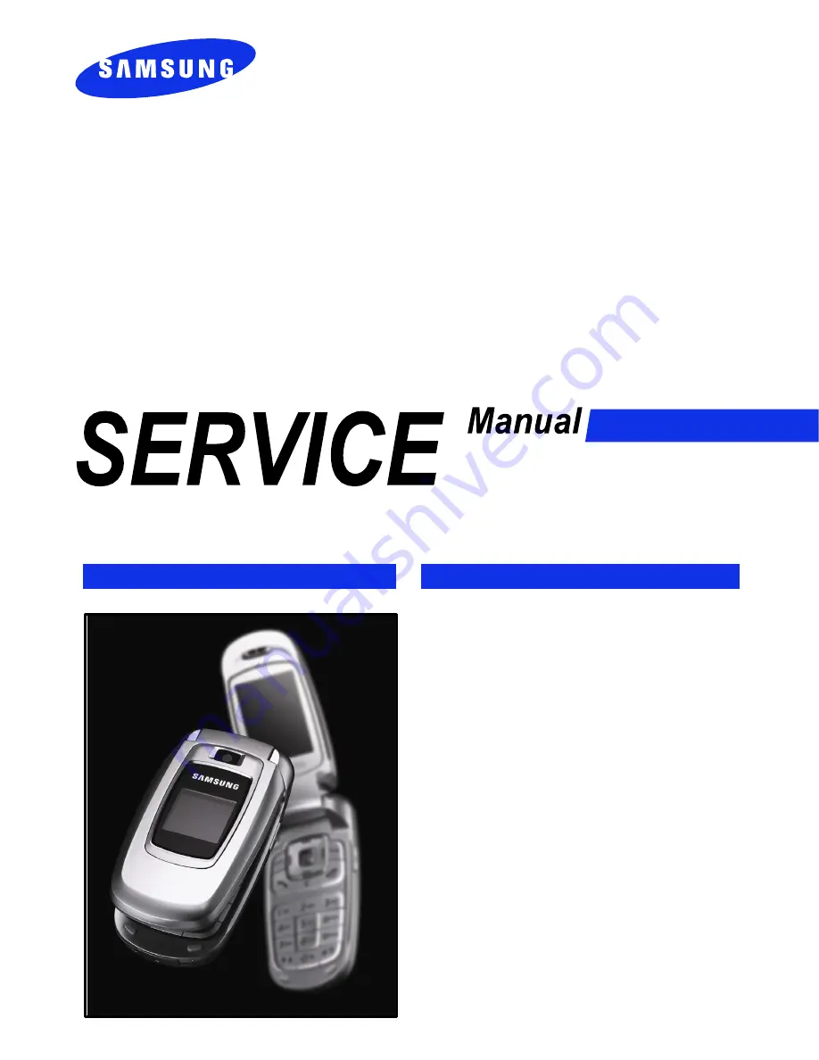
GSM TELEPHONE
SGH-X670
CONTENTS
1.
Specification
2.
Circuit Description
3.
Exploded Views and Parts List
4.
Electrical Parts List
5.
Block Diagrams
6.
PCB Diagrams
7.
Flow Chart of Troubleshooting
8.
Exploded and assembling View
Page 1: ...H X670 GSM TELEPHONE CONTENTS 1 Specification 2 Circuit Description 3 Exploded Views and Parts List 4 Electrical Parts List 5 Block Diagrams 6 PCB Diagrams 7 Flow Chart of Troubleshooting 8 Exploded and assembling View ...
Page 2: ...o Ltd April 2006 Printed in Korea Code No GH68 09954A BASIC This Service Manual is a property of Samsung Electronics Co Ltd Any unauthorized use of Manual can be punished under applicable International and or domestic law ⓒ ...
Page 3: ...k Downlink 890 915 935 960 880 915 925 960 1710 1785 1805 1880 ARFCN range 1 124 0 124 975 1023 512 885 Tx Rx spacing 45MHz 45MHz 95MHz Mod Bit rate Bit Period 270 833kbps 3 692us 270 833kbps 3 692us 270 833kbps 3 692us Time Slot Period Frame Period 576 9us 4 615ms 576 9us 4 615ms 576 9us 4 615ms Modulation 0 3GMSK 0 3GMSK 0 3GMSK MS Power 33dBm 5dBm 33dBm 5dBm 30dBm 0dBm Power Class 5pcl 19pcl 5p...
Page 4: ...m 11 8 4dBm 12 6 4 dBm 13 4 4 dBm 14 2 5 dBm 15 0 5 dBm TX Power control level DCS1800 0 30 2 dBm 1 28 3 dBm 2 26 3 dBm 3 24 3 dBm 4 22 3 dBm 5 20 3 dBm 6 18 3 dBm 7 16 3 dBm 8 14 3 dBm 9 12 4 dBm 10 10 4 dBm 11 8 4dBm 12 6 4 dBm 13 4 4 dBm 14 2 5 dBm 15 0 5 dBm TX Power control level GSM900 5 33 2 dBm 6 31 3 dBm 7 29 3 dBm 8 27 3 dBm 9 25 3 dBm 10 23 3 dBm 11 21 3 dBm 12 19 3 dBm 13 17 3 dBm 14 1...
Page 5: ... dBm 16 11 5 dBm 17 9 5 dBm 18 7 5 dBm 19 5 5 dBm TX Power control level DCS1800 2 26 4 3 dBm 3 24 3 dBm 4 22 3 dBm 5 20 3 dBm 6 18 3 dBm 7 16 3 dBm 8 12 3 dBm 9 10 3 dBm 10 14 3 dBm 11 12 4 dBm 12 10 4 dBm 13 8 4dBm 14 6 4 dBm 15 4 4 dBm 1 3 GSM EDGE TX power class TX Power control level PCS1900 2 26 4 3 dBm 3 24 3 dBm 4 22 3 dBm 5 20 3 dBm 6 18 3 dBm 7 16 3 dBm 8 12 3 dBm 9 10 3 dBm 10 14 3 dBm ...
Page 6: ...SAMSUNG Proprietary Contents may change without notice This Document can not be used without Samsung s authorization Specification 1 4 ...
Page 7: ...n further amplifies the wanted channel output level to the desired value and rejects DC PAM PAM101 The module consists of two separated line ups one for low band LB 850 900 and one for high band HB 1800 1900 with input and output matching and internal power detection function and power control loop in GSM mode in GSM mode the internal power control circuit ensures a stable power output set by the ...
Page 8: ...ive die temperature Backlight Brightness Modulator The Backlight Brightness Modulator BBM contains a programmable Pulse width modulator PWM and FET to modulate the intensity of a series of LEDs or to control a DC DC converter that drives LCD backlight This phone SGH X670 use PWM control to contrast the backlight brightness Clock Generator The Clock Generator CG generates all clocks for internal an...
Page 9: ...ing process 2 2 8 Audio HFR_P and HFR_N from PCF5213EL1 are connected to the main speaker via analog switches MIC_P and MIC_N are connected to the main MIC as well EAR1 is the source of External Speaker YMU762 is a synthesizer LSI for mobile phones This LSI has a built in speaker amplifier for outputting sounds that are used by mobile phones in addition to game sounds and ringing melodies that are...
Page 10: ...O TCK for ARM and DSP core J SEL signal controls different access to ARM and DSP core ADC Analog to Digital Convertor receives the condition of temperature battery type and battery voltage 2 2 11 TOH2600DGI4KRA 26MHz TCX101 This system uses the 26MHz VCTCXO TOH2600DGI4KRA AFC control signal form PCF5213EL1 controls frequency from 26MHz x tal It generates the clock frequency This clock is connected...
Page 11: ...t can not be used without Samsung s authorization 3 Exploded View and Parts List 3 1 Exploded View QWD02 QFU01 QLC01 QCA01 QMO01 QSP01 QAN05 QFL01 QSC01 QCR04 QMW02 QFR01 QMI03 QKP01 QME01 QCA02 QMI01 QRE01 QIF01 QCR06 QBA01 QAN02 QRF01 QCK01 QRF03 QVO01 QVK01 QMP01 QCR05 ...
Page 12: ...H59 02873A QVK01 UNIT VOLUME KEY GH59 02874A QCA02 UNIT CAMERA KEY GH59 02875A QCA01 UNIT CAMERA GH59 02876A QRF03 PMO COVER EAR GH72 27157A QIF01 PMO COVER IF GH72 27165A QWD02 PCT WINDOW SUB GH72 27169A QMW02 PCT WINDOW MAIN GH72 27171A QRF01 MPR SHEET RF GH74 21697A QAN05 MEC INTENNA CONTACT GH75 08168A QFU01 MEC CASE UPPER FOLDER GH75 08684A QFL01 MEC CASE LOWER FOLDER GH75 08685A QRE01 MEC CA...
Page 13: ... USERS EU ITALIAN GH68 09437A CUSHION CASE 1 2 GH69 03629A BOX P SGHX670 EU GH69 03630A MPR BOHO VINYL LCD CONN GH74 15350A MPR SHEET FILTER LCD FPCB GH74 21694A MPR VINYL BOHO UPPER GH74 21700A MPR VINYL BOHO MAIN LCD GH74 21701A MPR VINYL BOHO LOWER GH74 21702A MPR CUSHION LCD GH74 22342A MPR TAPE FOAM CAMERA GH74 22344A MPR TAPE INSULATION CAM CONN GH74 22611A MPR GASKET UPPER GH74 22612A MPR T...
Page 14: ...st 3 4 This Document can not be used without Samsung s authorization 3 3 Test Jig GH80 03306A 3 3 2 RF Test Cable GH39 00283A 3 3 3 Test Cable GH39 00337A 3 3 5 Power Supply Cable 3 3 6 DATA CABLE GH39 00331A 3 3 7 TA GH44 00482A 3 3 1 USB JIG Cable 3 3 4 Serial Cable CSA LL64151 A ...
Page 15: ... 000854 SA C131 C CER CHIP 2203 000854 SA C132 C CER CHIP 2203 000254 SA C134 C CER CHIP 2203 005444 SA C136 C CER CHIP 2203 000530 SA C137 C CER CHIP 2203 000233 SA C142 C CER CHIP 2203 000278 SA C143 C CER CHIP 2203 000278 SA C144 C CER CHIP 2203 000812 SA C200 C CER CHIP 2203 006562 SA C201 C CER CHIP 2203 005482 SA C202 C CER CHIP 2203 000254 SA C203 C CER CHIP 2203 005482 SA C204 C CER CHIP 2...
Page 16: ...TA CHIP 2404 001381 SA C411 C CER CHIP 2203 000812 SA C412 C CER CHIP 2203 006208 SA C413 C CER CHIP 2203 006562 SA C414 C CER CHIP 2203 006208 SA C415 C CER CHIP 2203 006257 SA C416 C CER CHIP 2203 006257 SA C418 C CER CHIP 2203 006825 SA C419 C CER CHIP 2203 005482 SA C421 C CER CHIP 2203 001153 SA C422 C CER CHIP 2203 006208 SA C423 C CER CHIP 2203 006208 SA C424 C CER CHIP 2203 006257 SA C425 ...
Page 17: ...C CER CHIP 2203 005683 SA C716 C CER CHIP 2203 005683 SA C717 C CER CHIP 2203 005683 SA C718 C CER CHIP 2203 005683 SA C719 C CER CHIP 2203 005683 SA C720 C CER CHIP 2203 005683 SA C721 C CER CHIP 2203 005683 SA C722 C CER CHIP 2203 005683 SA C723 C CER CHIP 2203 005683 SA D100 DIODE TVS 0406 001231 SA D600 DIODE TVS 0406 001231 SA D601 DIODE TVS 0406 001231 SA D602 DIODE TVS 0406 001231 SA D603 D...
Page 18: ...A L400 BEAD SMD 3301 001120 SA L401 INDUCTOR SMD 2703 002840 SA L500 BEAD SMD 3301 001534 SA L600 BEAD SMD 3301 001438 SA L601 BEAD SMD 3301 001438 SA L603 INDUCTOR SMD 2703 001231 SA L604 INDUCTOR SMD 2703 001673 SA L605 INDUCTOR SMD 2703 002206 SA L606 BEAD SMD 3301 001756 SA L607 BEAD SMD 3301 001756 SA L608 BEAD SMD 3301 001756 SA LED700 LED 0601 002055 SA LED701 LED 0601 002055 SA LED702 LED ...
Page 19: ... 2007 000162 SA R302 R CHIP 2007 000171 SA R303 R CHIP 2007 000155 SA R304 R CHIP 2007 000171 SA R305 R CHIP 2007 000137 SA R306 R CHIP 2007 001329 SA R307 R CHIP 2007 000162 SA R308 R CHIP 2007 000148 SA R309 R CHIP 2007 000162 SA R310 R CHIP 2007 000171 SA R311 R CHIP 2007 000141 SA R312 R CHIP 2007 000141 SA R313 R CHIP 2007 007014 SA R314 R CHIP 2007 001303 SA R315 R CHIP 2007 007014 SA R316 R...
Page 20: ...SA R701 R CHIP 2007 007009 SA R702 R CHIP 2007 007009 SA R703 R CHIP 2007 007009 SA R704 R CHIP 2007 007009 SA R705 R CHIP 2007 007009 SA R706 R CHIP 2007 007009 SA R707 R CHIP 2007 007009 SA R708 R CHIP 2007 007009 SA R709 R CHIP 2007 007009 SA R710 R CHIP 2007 007009 SA R711 R CHIP 2007 007009 SA R713 R CHIP 2007 000171 SA R715 R CHIP 2007 000170 SA R716 R CHIP 2007 000138 SA R717 R CHIP 2007 00...
Page 21: ...NALOG MULTIPLEX 1001 001345 SA U603 IC DEMODULATOR 1204 002398 SA U604 IC ANALOG SWITCH 1001 001231 SA U610 IC ANALOG SWITCH 1001 001362 SA U700 IC POSI FIXED REG 1203 003531 SA UCP200 IC COMM CONTROLLER 1205 002670 SA UME303 IC MCP 1108 000062 SNA V400 VARISTOR 1405 001082 SA V401 DIODE TVS 0406 001231 SA V500 THERMISTOR NTC 1404 001221 SA VR100 VARISTOR 1405 001082 SA ZD500 DIODE ZENER 0403 0015...
Page 22: ...SAMSUNG Proprietary Contents may change without notice Electrical Parts List 4 8 This Document can not be used without Samsung s authorization ...
Page 23: ...SAMSUNG Proprietary Contents may change without notice This Document can not be used without Samsung s authorization 5 Block Diagrams 5 1 5 1 RF Solution Block Diagram ...
Page 24: ...SAMSUNG Proprietary Contents may change without notice Block Diagrams This Document can not be used without Samsung s authorization 5 2 5 2 Base Band Solution Block Diagram ...
Page 25: ...SAMSUNG Proprietary Contents may change without notice 6 PCB Diagrams 6 1 This Document can not be used without Samsung s authorization 6 1 PCB Top Diagram ...
Page 26: ...SAMSUNG Proprietary Contents may change without notice PCB Diagrams 6 2 This Document can not be used without Samsung s authorization 6 2 PCB Bottom Diagram ...
Page 27: ...eck the clock generation circuit related to U100 Check for the clock at C312 26MHz Yes No Check the VDD_GSM_CORE circuit C401 VDD_GSM_CORE 1 8V Yes No Check the related circuit C425 VDD_IO_LOW C424 VDD_IO_HIGH H Yes No Resolder OSC400 Check the Clock at R402 32KHZ Yes No Check the PMU related to VINT C408 VINT 2 7V Yes No END Change the Battery Power On does not work Check the Battery Voltage is m...
Page 28: ...IRQ 10 _ONKEY 27 _REC1 1 _REC2 13 _RSTHC 11 44 _SIMRSCD SIMCKHC 8 SIMD3VBAT 40 SIMEN 45 SIMIOCD 42 SIMIOHC 9 SIMVCC 41 VBAT 31 VCHG 32 RF12VBAT 23 22 RF1VDD RF2VDD 24 SCL 2 SCN 38 SCP 37 SDA 3 SIMCKCD 43 MICBIAS 12 NC 53 54 NC OSCI 26 OSCO 25 PWREN1 6 PWREN2 5 REFC 28 GPO2 47 46 GPO3 18 HCVBAT HCVDD 17 IOD2VBAT 15 14 IOVDD 20 LPD1VBAT LPVDD 19 D1VDD 21 16 D2VDD D3VDD 39 GND 49 50 GND GND 51 52 GND...
Page 29: ...f Troubleshooting This Document can not be used without Samsung s authorization 7 3 7 2 Initial Q300 pin 4 RSTON H Initial Failure Check the circuit related to reset END No Yes Is UCP200 R214 R215 OK Yes Yes No Check the UCP200 Check the 16bit data signal memory CE Yes ...
Page 30: ...ICN L17 ANR L18 AUXADC5 L2 K2 AUXADC4 L1 GPIOA5 L11 AUXADC2 K1 EAR1 K15 ANL K18 AUXADC3 EAR2 J15 HFR1 J17 AUXADC1 J1 USBDP H11 HFR2 H18 RESET H1 GPIOA9 G1 USBDM G14 SIMCLK G17 USBCN F14 SIMRST F17 DCL E11 FSC D13 SIMIO D15 B14 DD B13 DU UCP200 R214 R207 R213 R208 VDD_IO_HIGH C222 VDD_IO_LOW KEY_LED_ON EAR1 EAR2 CHG_ON IT_PMU RX_TX_QN EDGE1_PA PON_SW RX_TX_QP RX_TX_IP SCL RF_CLK RX_TX_IN D_REF_CLK ...
Page 31: ...SAMSUNG Proprietary Contents may change without notice Flow Chart of Troubleshooting This Document can not be used without Samsung s authorization 7 5 ...
Page 32: ...w Chart of Troubleshooting 7 6 7 3 Charging Part Yes Resolder or replace U502 Check the circuit related to AUX_ON signal Resolder or replace U502 Check the circuit related to V_EXT_CHARGE Yes No Check the U502 pin 10 4 2V Yes No U502 pin 3 L Yes No U502 pin 5 L Yes No END Abnormal charging part Check the U502 pin 1 4 9V ...
Page 33: ...be used without Samsung s authorization 7 7 5 0V Typical 3 7V Typical 1 4V BATTERY CHARGING R515 C504 VBAT R510 ZD500 R511 C503 ZD501 C506 R514 R512 C505 VDD_IO_HIGH _EN 5 3 _PPR CRDL 1 11 GND GND 8 9 ICDL 6 IMIN USB 2 USBON 7 _CHG 4 U502 BAT 10 VBUS V_EXT_CHARGE USB_CHG_ON END_OF_CHG AUX_ON MES_BATT CHG_ON ...
Page 34: ...zation Flow Chart of Troubleshooting 7 8 7 4 Sim Part SIM400 pin 1 5 H Phone can t access SIM Card Check the sim charge pump Check the SIM Card END No Yes Yes Yes No Check the Clock After Power ON Check SIMCLK Signal on pin3 of SIM400 in a few Yes No Replace PBA After SIM card insert SIM400 pin 2 H SIM_RST Yes ...
Page 35: ...IO_LOW TP400 BAT400 NEG POS _SIMRSHC 7 VINT 29 VSAVE 30 _REC1 1 44 _SIMRSCD SIMCKHC 8 SIMD3VBAT 40 SIMEN 45 SIMIOCD 42 SIMVCC 41 VBAT 31 VCHG 32 SCL 2 SCN 38 SCP 37 SDA 3 SIMCKCD 43 NC 53 54 NC PWREN1 6 PWREN2 5 REFC 28 GPO2 47 46 GPO3 D3VDD 39 GND 49 50 GND GND 51 52 GND GPO1 48 U400 CHGCUR BATMAX 34 CHGDRV 33 CLK32K 4 CPVBAT 36 CPVDD 35 R401 G 9 10 G 1 2 3 4 5 6 G 7 8 G SIM400 C409 PON_TX BU_RST...
Page 36: ...Chart of Troubleshooting 7 10 7 5 Microphone Part Replace the MIC No Check the MIC Yes Microphone does not work Check the JACK_IN JACK_EN signal No Check R605 R625 H No Yes Yes Yes Yes No END Resolder the C603 C606 R601 R603 R604 L600 L601 U600 Resolder MIC Check the circuit from UCP200 to MIC Check the connection from MIC ...
Page 37: ...601 L608 L607 C615 L606 C612 G 99 G 11 12 G G 13 14 G 15 G G 16 G 17 18 10 2 2 33 4 4 55 6 6 77 8 8 EAR600 11 10 C602 C608 R602 C604 C606 C603 R625 D600 R612 R607 L603 VDD_IO_HIGH C617 1 2 3 4 5 6 ZD601 D601 C600 R600 MIC_BIAS_BB 2 NO1 NO2 10 VCC 1 MIC_BIAS COM1 3 COM2 9 GND 6 IN1 4 IN2 8 5 NC1 7 NC U600 C611 R603 MIC600 C607 C601 C605 L600 D603 L601 R605 R606 EARSPK_L HFR_N EARSPK_R JACK_IN MIC_N...
Page 38: ...dy Check the U602 Pin 3 15 Speaker does not work Check the U604 Pin 5 EAR1 Check the U604 Pin 1 LOUD_EN Resolder U604 No Yes No Check the U300 Yes U300 pin 17 18 1 8V When U300 operate Resolder U300 No Yes No END Check LCD MODULE SPK SPK Operate Check the board to board Connector Is Speaker working Change the Speaker No Yes Yes Yes Check the C705 C706 Resolder U602 No Yes ...
Page 39: ... VBAT C722 Y 2 Y 1 Y 0 M_CLK PCLK HSYNC VSYNC M_SCL M_SDA SPK_P SPK_N DIM_EN Y 7 Y 6 Y 5 Y 4 Y 3 Typical 3 7V VBAT 13 NC4 NC 22 21 NC 15 NO1 3 NO2 NO3 7 11 NO4 V 14 COM4 12 GND 6 GND 17 2 IN1 IN2 IN3 IN4 10 1 NC1 NC2 5 NC3 9 U602 COM1 16 4 COM2 COM3 8 SPK_N SPK_P ANR AFR HPR AFL R_CONTROL AMP_N HFR_P AMP_P MELODY_SEL HFR_N HPL ANL MELODY IC C311 C300 R304 VDD_IO_LOW C306 C304 R306 R305 C305 R300 R...
Page 40: ...SAMSUNG Proprietary Contents may change without notice This Document can not be used without Samsung s authorization Flow Chart of Troubleshooting 7 14 ...
Page 41: ...02 pin 1 5 1 5V Resolder UCP200 or change PBA END No Yes Yes Receiver does not work LCD MODULE SPK PAD 1 5V Change the Board to Board Connector No Yes Is Receiver working Replace the Speaker No Yes No Resolder or replace U602 Yes No change UCP200 HDC700 pin 49 51 1 5V Yes Check the soldering of the spaeaker wire No Modify the speaker wire soldering Yes U602 pin 4 16 1 5V ...
Page 42: ... Troubleshooting 7 16 7 8 Key Data Input When one of the keys is pushed Isn t it displayed on LCD Check the Dome sheet Key Pad END No Yes Yes Check Initial Operation When one of the keys is pushed KEY_ROW 0 4 KEY_COL 0 4 signal is OK Check the D702 D715 Direction Replace Volume Key FPCB or Camera Key FPCB or Replace the PBA No Yes ...
Page 43: ...GIT1 12 DIGIT9 12 DIGIT6 R717 DIGIT4 12 DIGIT8 12 DOWN 12 SIDE_KEY VK700 4 GND 3 V_COMMON V_DOWN 2 1 V_UP D710 2 LEFT 12 RIGHT 1 12 DIGIT5 D713 D704 CK701 CAMERA_KEY GND 3 IN 1 OUT 2 D700 12 UP 12 CLR R719 R720 2 SOFT2 1 12 12 D711 DIGIT3 DIGIT7 D715 D705 D714 R716 2 D706 END 1 D708 D709 D707 SHARP1 12 R718 KEY_COL 1 KEY_COL 0 KEY_ROW 3 ONKEYN KEY_COL 0 KEY_COL 1 KEY_COL 2 KEY_COL 3 KEY_COL 4 KEY_...
Page 44: ...ow Chart of Troubleshooting 7 18 7 9 Back Light for Color Main LCD Is LCD Contrast set on high level in the Menu Set LCD Contrast on high level END No Yes Yes Backlight does not work IC3 pin 2 H Change the board to board Connector No Yes IC3 PIN 5 VBAT Check the IC3 the related circuit No Yes Yes Replace the LCD Module ...
Page 45: ...SAMSUNG Proprietary Contents may change without notice Flow Chart of Troubleshooting This Document can not be used without Samsung s authorization 7 19 ...
Page 46: ...20 7 10 Key Back Light U700 pin6 H Check the UCP200 related to KEY_LED_ON END No Yes Yes Main Key LED does not work Typical 3 7V KEY_LED R708 R707 R705 R706 R704 LED708 LED700 LED707 LED702 R710 R711 R709 VBAT LED709 LED706 LED701 LED705 LED704 2 NC 4 NC 1 VIN VOUT 3 5 VSS U700 6 CE GND 7 R703 R701 R702 R700 LED703 C700 C701 LED710 LED711 KEY_LED_ON ...
Page 47: ...amsung s authorization 7 21 7 11 Camera part Camera function does not work Yes No Reconnect the camera module Check the Camera Connector Yes J2 Pin 3 26 2 9V IC2 Pin 5 1 8V No Check the U400 or IC2 Yes R314 26MHz No Check U302 pin2 pin4 related to 26Mhz and R314 Yes Is there another problem END Replace the camera module Yes ...
Page 48: ...SAMSUNG Proprietary Contents may change without notice This Document can not be used without Samsung s authorization Flow Chart of Troubleshooting 7 22 ...
Page 49: ...8 K10 LD5 LD6 K9 K8 L6 LD0 M10 M9 LD1 J8 LD10 LD11 H8 G9 LD12 G8 LD13 F9 LD14 LD15 D8 C5 GPIO4 C4 GPIO5 C2 GPIO6 GPIO7 MD17 B2 B1 GPIO8 MD16 A9 HREF K6 LCS1 LCS2 DVSS DVSS F10 H9 DVSS J10 DVSS K2 DVSS DVSS L5 GPIO0 E9 GPIO1 D10 GPIO2 DI6 A6 B7 DI7 DVSS2 C8 DVSS M8 B3 DVSS DVSS A7 D3 DVSS DVSS C9 F3 L4 L7 CVDD DI0 A3 B4 DI1 DI2 A4 B5 DI3 DI4 A5 B6 DI5 U305 CLKI G10 CLKO H10 CVDD C6 CVDD E10 CVDD R3...
Page 50: ...ment can not be used without Samsung s authorization Flow Chart of Troubleshooting 7 24 7 12 FM RADIO FM Radio function does not work Yes No Insert the Earphone or Change the Earphone Check the Insert Earphone Yes R624 2 9V No Check the U400 Yes END Replace the U603 ...
Page 51: ...VDD_IO_HIGH C624 R624 MPXOUT G5 VAFR G6 TMUTE G7 INTX F1 XTAL F2 AGND F4 VAFL F6 INTCON1 F7 DGND G1 FREQIN G2 TIFCENTER G3 NC G4 C7 DGND D1 RFIN1 D2 CD3 D6 DGND D7 VDD E1 VCC E6 INTCON2 E7 CD2 A7 CLOCK B1 CAGC B2 CPOUT B4 NC B6 VREFDIG B7 DATA C1 RFIN2 C2 RFGND 1 NC 2 NC A1 LOOPSW A2 LO1 A3 LO2 A4 CD1 A5 SWPORT A6 BUSENABLE U603 C618 L605 C627 R618 C625 C628 BUSENABLE SW_PORT AFL AFR R_INT SCL SDA...
Page 52: ...y change without notice This Document can not be used without Samsung s authorization Flow Chart of Troubleshooting 7 26 7 13 BLUETOOTH R316 H Check the UCP200 END No Yes Yes BLUETOOTH does not work Replace ANT300 Yes Replace U301 No ...
Page 53: ...5 TP317 TP311 L300 TP313 TP314 C314 SPIMISO F2 SPICSB F3 PIO2 F4 GND F5 GND D6 SPIMOSI E1 SPICLK E2 PIO4 E3 PIO1 E4 GND E5 RF_IO E6 GND F1 AIO0 C4 RESETB C5 VDD18V C6 PCMCLK D1 PCM_IN D2 PIO5 D3 PIO0 D4 PIO3 D5 UART_RxD B2 UART_CTS USB B3 PIO8 B4 VCC_IO B5 VCC B6 PCM_OUT C1 PCM_SYNC C2 GND C3 NC NC 2 NC A2 X_IN A3 UART_RTS USB A4 GND A5 GND A6 UART_TxD B1 U301 TP316 TP312 TXD2 RXD2 DU FSC DCL DD B...
Page 54: ... RFS101 C106 No Yes RX ON RF input 62CH Amp 50dBm Check LMSP54HA 350 pin9 pin10 pin12 L LMSP54HA 350 pin5 pin6 65dBm Check ANT Switch control circuit Resolder Module1 Yes Yes No No END U102 pin7 8 9 10 1V U102 pin30 70dBm pin29 70dBm Resolder C117 C119 L111 Check U102 pin28 pin31 2 7V Check Resolder U102 R108 R107 RF26MHz RF PSU Part Resolder U102 C140 C141 1V Yes Yes Yes Yes Yes No No No Check UC...
Page 55: ...0 H 2 68V pin9 pin12 L LMSP54HA 350 pin11 18dBm PAM101 18pin 18dBm PAM101 14pin 11dBm Change or Resolder LMSP54HA 350 Check ANT Switch control circuit Resolder L115 C134 Yes Check PAM101 VBAT pin15 pin8 OK Resolder or Change PAM101 Check VBAT or PAM101 control signal No No No No Yes Yes Yes Yes Yes No Yes No No No Check Resolder U102 R108 R107 RF26MHz RF PSU Part Check U102 pin28 pin31 2 7V OK U10...
Page 56: ...RFS101 C106 No Yes RX ON RF input 698CH Amp 50dBm Check Module1 pin9 pin10 pin12 L LMSP54HA 350 pin1 pin2 65dBm U102 pin35 70dBm pin36 70dBm Check ANT Switch control circuit Resolder LMSP54HA 350 Resolder C112 C115 L110 Yes Yes Yes No No No END U102 pin7 8 9 10 1V Check U102 pin28 pin31 2 7V Check Resolder U102 R108 R107 RF26MHz RF PSU Part Resolder U102 C140 C141 1V Yes Yes Yes Yes No No Check UC...
Page 57: ...12 H 2 68V pin9 pin10 L LMSP54HA 350 pin13 18dBm PAM101 pin20 18dBm PAM101 pin4 11dBm Change or Resolder Module1 Check ANT Switch control circuit Resolder L116 C144 Yes Check PAM101 VBAT pin3 pin8 OK Resolder or Change PAM101 Check VBAT or PAM101 control signal No No No No No Yes Yes Yes Yes Yes No Yes U102 pin7 8 9 10 1V Check Resolder U102 R108 R107 RF26MHz RF PSU Part Yes No No END Check UCP200...
Page 58: ...FS101 C106 No Yes RX ON RF input 661CH Amp 50dBm Check LMSP54HA 350 pin9 H pin10 pin12 L LMSP54HA 350 pin3 pin4 65dBm U102 pin32 70dBm pin33 70dBm Check ANT Switch control circuit Resolder LMSP54HA 350 Resolder C142 C143 Yes Yes Yes No No No END U102 pin7 8 9 10 1V Check U102 pin28 pin31 2 7V Check Resolder U102 R108 R107 RF26MHz RF PSU Part Resolder U102 C140 C141 1V Yes Yes Yes Yes No No Check U...
Page 59: ...12 H 2 68V pin9 pin10 L LMSP54HA 350 pin13 18dBm PAM101 pin20 18dBm PAM101 pin4 11dBm Change or Resolder LMSP54HA 350 Check ANT Switch control circuit Resolder L116 C144 Yes Check PAM101 VBAT pin3 pin8 OK Resolder or Change PAM101 Check VBAT or PAM101 control signal No No No No No Yes Yes Yes Yes Yes No Yes U102 pin7 8 9 10 1V Check Resolder U102 R108 R107 RF26MHz RF PSU Part Yes No No END Check U...
Page 60: ...9 C104 R114 C141 L112 VDAC 8 VREF 13 VSTAB 9 4 RFIN_LB 14 RFOUT_HB 20 RFOUT_LB 18 TXON 7 2 VBAT VBAT 3 16 VBAT VBAT 15 10 GND 1 GND 17 GND 21 MODE 5 NC 6 NC 11 NC 12 RFIN_HB PAM101 GND 19 BAND C133 R122 R121 C137 R120 L110 L113 L117 C102 VCC_SYN L101 L106 L115 C142 C115 R116 C124 R113 R108 C106 R106 R124 L116 C101 C139 C105 C132 R119 L119 R117 C107 TA101 1 1 2 2 3 3 4 4 5 5 6 6 R109 ANT101 ANTCON ...
Page 61: ...SAMSUNG Proprietary Contents may change without notice Flow Chart of Troubleshooting This Document can not be used without Samsung s authorization 7 35 ...
Page 62: ...SAMSUNG Proprietary Contents may change without notice This Document can not be used without Samsung s authorization Flow Chart of Troubleshooting 7 36 ...
Page 63: ...t be used without Samsung s authorization Disassembling Procedure Loosen the Rear Screw Disassemble the Folder Ass y and the Rear from the bottom of side Separate the Folder Ass y and the Rear Take out the Ear Cover and separate the LCD Connector Separate the PBA and the Folder Ass y Remove the Tape 1 2 3 4 5 6 ...
Page 64: ...nt can not be used without Samsung s authorization Take out the Keypad Separate the Folder and the Front Detach the Folder Screw Cap and loosen the Folder Screw Disassemble the Folder from the bottom Separate the Folder Lower and Folder Upper Separate the Folder Lower and the LCD Ass y 12 11 10 9 7 8 ...
Page 65: ... Attach the Domesheet on the PBA according to Guide Hole Resolder the Volume Key and the Camera Key Resolder the Mic Attach the Insulated Tape 2 POINT and the Conducted Tape 1 POINT Attach the Paper Tape Bond the Motor and Speaker after resoldering with attention to polarity 1 2 3 4 5 6 GUIDE HOLE GUIDE HOLE GUIDE HOLE GUIDE HOLE INSULATED TAPE CONDUCTED TAPE PAPER TAPE ...
Page 66: ...amsung s authorization Attach the Main Window on the Folder Lower Put the Camera in the Folder Lower Put the LCD Ass y in the Folder Lower Attach the Insulated Tape and Sponge on the LCD Ass y Attach the Sub Window on the Folder Upper Assemble the Folder from the top 7 8 9 10 11 12 CAMERA ARRANGE the WIRE SPONGE INSULATED TAPE ...
Page 67: ...ew 8 5 This Document can not be used without Samsung s authorization Tighten the Folder Screws Attach the Screw Cap Assemble the Folder and the Front Insert the Keypad Attach the Tape to prevent indraft of dust Assemble the Intenna on the Rear and tighten the Screw 18 17 15 16 14 13 ...
Page 68: ...y change without notice Exploded and assembling View 8 6 This Document can not be used without Samsung s authorization Insert the PBA and join the LCD Connector Assemble the Folder Ass y and the Rear Tighten the Rear Screws 22 21 20 ...