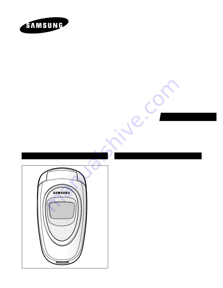
SGH-X460
SERVICE
Manual
GSM TELEPHONE
CONTENTS
1.
Specification
2.
Circuit Description
3.
Exploded Views and Parts List
4.
Electrical Parts List
5.
Block Diagrams
6.
PCB Diagrams
7.
Flow Chart of Troubleshooting
Page 1: ... SERVICE Manual GSM TELEPHONE CONTENTS 1 Specification 2 Circuit Description 3 Exploded Views and Parts List 4 Electrical Parts List 5 Block Diagrams 6 PCB Diagrams 7 Flow Chart of Troubleshooting GSM TELEPHONE ...
Page 2: ...onics Co Ltd May 2004 Printed in Korea Code No GH68 05344A BASIC ⓒ This Service Manual is a property of Samsung Electronics Co Ltd Any unauthorized use of Manual can be punished under applicable International and or domestic law ...
Page 3: ...805 1880 ARFCN range 1 124 0 124 975 1023 512 885 Tx Rx spacing 45MHz 45MHz 95MHz Mod Bit rate Bit Period 270 833kbps 3 692us 270 833kbps 3 692us 270 833kbps 3 692us Time Slot Period Frame Period 576 9us 4 615ms 576 9us 4 615ms 576 9us 4 615ms Modulation 0 3GMSK 0 3GMSK 0 3GMSK MS Power 33dBm 13dBm 33dBm 5dBm 30dBm 0dBm Power Class 5pcl 15pcl 5pcl 19pcl 0pcl 15pcl Sensitivity 102dBm 102dBm 100dBm ...
Page 4: ...2 dBm 7 29 2 dBm 8 27 2 dBm 9 25 2 dBm 10 23 2 dBm 11 21 2 dBm 12 19 2 dBm 13 17 2 dBm 14 15 2 dBm 15 13 2 dBm 16 11 3 dBm 17 9 3dBm 18 7 3 dBm 19 5 3 dBm TX Power control level DCS1800 0 30 3 dBm 1 28 3 dBm 2 26 3 dBm 3 24 3 dBm 4 22 3 dBm 5 20 3 dBm 6 18 3 dBm 7 16 3 dBm 8 14 3 dBm 9 12 4 dBm 10 10 4 dBm 11 8 4dBm 12 6 4 dBm 13 4 4 dBm 14 2 5 dBm 15 0 5 dBm 2 GSM TX power class ...
Page 5: ... the logic and RF After additional process the reference clock applies to the U100 Rx IQ demodulator and Tx IQ modulator The oscillator for RX IQ demodulator and Tx modulator are controlled by serial data to select channel and use fast lock mode for GPRS high class operation 5 UAA3536 U100 This chip integrates two differential input LNAs The GSM input supports the E GSM DCS input supports the DCS1...
Page 6: ...erter provides support for 1 8V 3 0V and 5 0V SIMs while a self resetting electronically fused switch supplies power to external accessories Ancillary support functions such as RTC module and High Voltage Charge pump Clock generator aid in reducing both board area and system complexity I2C BUS serial interface provides access to control and configuration registers This interface gives a microproce...
Page 7: ...from OM6357 are used for audio speaker And VDD_VIB from PCF50601 enables the motor 2 Key This is consisted of key interface pins among OM6357 KBIO 0 7 These signals compose the matrix Result of matrix informs the key status to key interface in the OM6357 Power on off key is separated from the matrix So power on off signal is connected with PCF50601 to enable PCF50601 twelve key LED use the VBAT su...
Page 8: ...ly support application such as incoming call melody music distribution service The hardware sequencer built in this device allows playing of the complex music without giving excessive load to the CPU of the portable telephones Moreover the registers of the FM synthesizer can be operated directly for real time sound generation allowing for example utilization of various sound effects when using the...
Page 9: ...AM in the ARM core DSP is consisted of KBS JTAG EMI and UART ARM core is consisted of EMI PIC Programmable Interrupt Controller reset power clock unit DMA controller TIC Test Interface Controller eripheral bridge PPI SSI Synchronous Serial Interface ACC Asynchronous communications controllers timer ADC RTC Real Time Clock and keyboard interface KBIO 0 7 address lines of DSP core and HD 0 15 HA 1 2...
Page 10: ...X460 Exploded View and its Parts list 3 1 This Document can not be used without Samsung s authorization 1 Cellular phone Exploded View 1 QFU01 QMO02 QSP04 QFL01 QMW01 QCR04 QSC11 QKP01 QFR01 QMP01 QME02 QAN02 QRE01 QRF01 QCR04 QVO01 QIF01 QBA18 QVK01 QLC67 QSC12 ...
Page 11: ...1574 QMO02 MOTOR 3101 001315 QFL01 FOLDER LOWER GH75 04525A QMW01 MAIN WINDOW LCD GH75 04528A QFR01 FRONT COVER GH75 04523A QVO01 VOLUME KEY GH75 04529A QKP01 KEYPAD GH75 04527A QMP01 MAIN PBA GH92 01799A QVK01 VOL KEY FPCB GH59 01419A QAN02 INTENNA GH42 00425A QME02 METAL DOME GH59 01418A QRE01 REAR COVER GH75 04526A QIF01 IF COVER GH72 13265A QRF01 RF COVER GH72 15078A QCR04 SCREW 6001 001479 QB...
Page 12: ...loded view and its Part list 3 3 This Document can not be used without Samsung s authorization 3 Test Jig GH80 01909A 3 1 RF Test Cable GH39 00261A 3 2 Test Cable GH39 00217A 3 3 Serial Cable 3 4 Power Supply Cable 3 5 DATA CABLE GH39 00143B 3 6 TA GH44 00482A ...
Page 13: ... 2007 000146 R308 2007 000148 R107 R118 R121 R124 2007 000148 R132 R133 R201 R400 2007 000148 R401 R504 2007 000157 R312 R316 2007 000162 R200 R202 R203 R303 2007 000162 R306 R307 R313 R315 SEC CODE Design LOC 2007 000162 R317 R323 R324 R501 2007 000162 R600 R601 2007 000171 R102 R105 R111 R112 2007 000171 R207 R305 R403 R532 2007 000172 R103 2007 000173 R507 R509 R510 R511 2007 000173 R512 R513 R...
Page 14: ...05 2203 005482 C206 C208 C209 C210 2203 005482 C211 C212 C213 C214 2203 005482 C215 C216 C217 C218 2203 005482 C219 C220 C301 C304 2203 005482 C306 C309 C312 C319 2203 005482 C401 C403 C404 C408 2203 005482 C414 C417 C428 C504 2203 005482 C505 C509 2203 006053 C124 C308 C421 C424 SEC CODE Design LOC 2203 006053 C425 C426 C427 2203 006093 C411 C524 2203 006137 C307 2203 006208 C402 C406 C413 2203 0...
Page 15: ...ET Mixer input power 16dBm max 22dBm min fcompRF 26MHz Philips Transceiver UAA3536 Pins IA IB QA and QB V I Q 1 25V ty p 1 15V mi n 1 35Vmax Vmod 0 5V p p VC1 VC2 QUA D FUJITSU DCS RX SAW Filter FAR F6EB 1G8425 B2BC IL 3 3dB max Ripple 2 0dB max DIV PFD CP VREG Vcc_RF_LO Frac N DIV 1 1 2 VREG 26MH z Vcc_REF 2 4V typ Vcc_SYN FESW1 FESW2 3W BUS CT L RE G PWR EN GSM DCS DIV QUA D PFD CP fTXIF 60 114M...
Page 16: ...Battery Temperature AFC RAMP Charging Circuit Li Ion Battery Slim OM6357 VIBRATOR SYSTEM CLOCK 26MHz RTC_CLOCK 32 768KHz KEY_BOARD RECEIVER MIC LCD RF INTERFACE VCC_RX_TX VCC_RF_VCO VCC_TX_BURST PMU VCC_SYN Serial Data Interface I O Interface A D Interface BB INTERFACE MELODY IC 40 Poly SPEAKER FLASH 256M bit VDD1 VDD2 VDD3 VDD_VIB MIC_BIAS VCC_CP VDD_KEY VDD_AMP AVDD AVDD_TEMP SIM CARD SRAM 32M b...
Page 17: ...SAMSUNG Proprietary Contents may change without notice 6 SGH X460 PCB Diagrams 6 1 This Document can not be used without Samsung s authorization 1 Main PCB Top Diagram ...
Page 18: ...SAMSUNG Proprietary Contents may change without notice PCB Diagrams 6 2 This Document can not be used without Samsung s authorization 2 Main PCB Bottom Diagram ...
Page 19: ...more than 3 4V Power On does not work Change the Battery END No Yes C410 V_ISUP 2 7V Check the PMU related to V_ISUP No Yes Check the Clock at R402 32KHZ Resolder X1 No Yes C427 VDD1 H Check the VDD1 circuit No Yes C426 VDD2 C425 VDD3 2 8V Check the VDD2 VDD3 circuit No Yes Check for the clock at C121 26MHz Check the clock generation circuit related to OSC101 No Yes Check the initial operation Yes...
Page 20: ...A2 SIMGND SIMIO B8 A1 SIMSCN B1 SIMSC P B2 SIMVBAT D1 0 SLPMOD H5 TM VBACK J5 G9 RFVBAT RST C1 RSTO D9 E3 SCL F2 SD A E9 SEL12RB H4 SEL3RB C6 F10 RF1SNS RF1SW S E8 G10 RF1VDD F9 RF1VDD S H9 RF2SNS E10 RF2SW S H10 RF2VDD J10 RF2VDD S NC ONKEY H3 OSC32I K8 OSC32O K9 K1 REC1 J2 REC2 K2 REC3 H8 REFC K6 REFGND D8 HVSVDD INT C10 D2 IO H6 ISUPA J4 ISUPD J6 MICBIAS 1 NC 2 HFAVBA T HFAVBA T B5 HFAVD D A6 B...
Page 21: ...bleshooting 7 3 This Document can not be used without Samsung s authorization 2 Initial Initial Failure Check the circuit related to reset END No Yes Is U303 pin 4 6 memory CE OK Yes Yes No Check the U303 Check the circuit around LCD U302 Short or not solder Yes R200 RSTON H ...
Page 22: ...8 L10 GPON 1 N9 GPON 2 CS_N 3 CTS0_N B5 EARN A11 B10 EARP GPIO 0 M1 2 K9 GPIO 1 K8 GPIO10 L8 GPIO 2 M9 CD O E9 CEN D9 P11 CKI CKI32I P13 P14 CKI32O CS_N 0 N4 G5 CS_N 1 CS_N 2 M5 G3 AVSS P10 BDIO E11 F10 BIEN BIOCLK F11 G11 BOEN BU Z B11 E10 CCLK D8 CD I AUXDAC3 D12 A14 AUXMICN AUXMIC P B14 AUXO N K14 A10 AUXSP AUXST G10 P1 2 AVD D AD I A8 A9 AD O B9 AFS AUXADC1 F14 G14 AUXADC2 AUXADC3 E14 F13 AUXA...
Page 23: ... without Samsung s authorization 3 Charging Part Check the U304 pin 2 4 9V Abnormal charging part END No Yes U304 pin 6 H No Yes U304 pin 5 CHG_ON L No Yes U304 pin 7 4 2V No Yes Check the the circuit related to CHARGER_OK Resolder or replace U304 Check the circuit related to CHG_ON signal Resolder or replace U304 Yes ...
Page 24: ...ry PCB_HOLE R322 3 100K 1 R320 220K R321 V300 NCP15WB473J04RC 100K 1 VDD2 47K R316 C314 10UF 6 3V AVDD_TEM P V304 10V C315 10UF C317 470nF C316 100PF UDZS8 2B ZD301 V301 VC040205X150R 2 7K R318 V302 VC040205X150R R319 330K 1 8 _EN 5 10 GG 11 12 G GND 3 IN 2 ISET 4 1 VL _ACO K 6 _CHG MAX1508ETA U304 7 BATT G 9 END_OF_CHARGE MES_BATT VBA T CHARGER_O K DCVOLT TEMP_PRODUCT CHG_ON ...
Page 25: ... be used without Samsung s authorization 4 Sim Part CN500 pin 1 5 H Phone can t access SIM Card Check the sim charge pump Check the SIM Card END No Yes Yes Yes No Check the 32k OSC After Power ON Check SIMCLK Signal on CN500 pin3 in a few second Yes No Replace PBA After SIM card insert CN500 pin 2 H SIM_RST Yes ...
Page 26: ...A2 SIMGND SIMIO B8 A1 SIMSCN B1 SIMSC P B2 SIMVBAT D1 0 SLPMOD H5 TM VBACK J5 G9 RFVBAT RST C1 RSTO D9 E3 SCL F2 SD A E9 SEL12RB H4 SEL3RB C6 F10 RF1SNS RF1SW S E8 G10 RF1VDD F9 RF1VDD S H9 RF2SNS E10 RF2SW S H10 RF2VDD J10 RF2VDD S NC ONKEY H3 OSC32I K8 OSC32O K9 K1 REC1 J2 REC2 K2 REC3 H8 REFC K6 REFGND D8 HVSVDD INT C10 D2 IO H6 ISUPA J4 ISUPD J6 MICBIAS 1 NC 2 HFAVBA T HFAVBA T B5 HFAVD D A6 B...
Page 27: ...his Document can not be used without Samsung s authorization 5 Microphone Part Check the connection from MIC Check the circuit from U200 to MIC Resolder MIC Resolder the R503 R505 C505 C509 R532 R502 and R506 END No Yes Yes Yes Yes No Check the MIC No Replace the MIC Microphone does not work ...
Page 28: ...501 C527 33UF 4V BLM10B750SBPT R503 BLM10A102SGPT L503 6 3V uClamp0501 H ZD504 C524 10UF 10PF 330PF C503 C510 R531 22 R517 22 LED507 LED508 22 R509 LED506 NC C525 22 R512 130K 1 R521 150K 1 R518 7 VDD2 C511 10PF U501 2 TC75W56FK TE12L 5 6 V502 uClamp0501H R504 10K ZD503 uClamp0501 H ZD505 uClamp0501 H ZD506 uClamp0501 H 100NF C532 ZD502 uClamp0501 H VDD2 R522 130K 1 LED511 22 R511 22 R510 uClamp05...
Page 29: ... U301 pin 5 2 85V Speaker does not work Check the Clock signal at Pin 1 of U302 13MHz Check the clock generation circuit related to OSC101 and U301 END No Yes No Resolder or replace U301 U302 pin 17 18 1 8V When U400 operate Resolder U302 Yes No CN600 pin 28 30 1 8V Check the circuit related to SPK_P SPK_N signal Yes No Is Speaker working No Yes Change the Speaker Yes Yes ...
Page 30: ...2 2 NC 1 OUT 4 VCC 5 TC7SH04FU TE85L U301 GND 3 IN R302 100N F C312 51K VDD2 C300 100PF VDD3 1NF C305 330 R301 100K VDD3 R323 100K R324 150PF C310 3 IRQ RD 31 RST 4 28 W R 17 SPOUT 1 SPOUT 2 18 15 SPVDD SPVSS 16 7 VDD VREF 9 VS S 8 C S 29 HPOUT L MONO 10 11 HPOUT R IOVDD 32 LED 2 19 MTR 5 NC PLLC 6 21 D6 20 D7 EQ 1 12 13 EQ 2 EQ 3 14 33 G G 34 35 G G 36 30 A0 1 CLKI D0 27 26 D1 25 D2 D3 24 23 D4 D...
Page 31: ...ting 7 13 This Document can not be used without Samsung s authorization 7 Key Data Input When one of the keys is pushed is it displayed on LCD Check the Dome sheet Key Pad END No Yes Yes Check Initial Operation When one of the keys is pushed KBIO signal is OK Replace the PBA No Yes ...
Page 32: ...eceiver Part U502 pin 3 8 12 15 1 5V Resolder or replace U502 END No Yes Yes Receiver does not work Check the soldering of the speaker wire Modify the speaker wire soldering No Yes No Resolder EAR500 Yes No Resolder EAR500 EAR500 pin 2 3 5 1 5V Yes CN600 pin 28 30 1 5V No Replace CN600 Yes Is Receiver working No Replace the Receiver Yes EAR500 pin 5 short ...
Page 33: ...an not be used without Samsung s authorization 9 Back Light for Color Main LCD Is LCD Contrast set on high level in the Menu Set LCD Contrast on high level END No Yes Yes Backlight does not work CN600 pin 24 2 8V Resolder R606 R323 No Yes CN600 pin 29 3 05V Replace the PBA No Yes Yes Replace the LCD Module ...
Page 34: ...ice Flow Chart of Troubleshooting 7 16 This Document can not be used without Samsung s authorization 10 Key Back Light U500 pin 3 H Check the PMU related to VDD_KEY END No Yes Yes Key Backlight does not work U500 pin 5 H No Resolder or replace U500 Yes ...
Page 35: ...lder CON101 L112 END No Yes RX ON RF input CH center freq 67 7kHz Amp 50dBm Check U102 pin7 L pin4 L U102 pin8 65dBm F100 pin1 70dBm U100 pin6 7 8 9 1V U100 pin32 70dBm pin33 70dBm Check ANT Switch control circuit Resoder U102 Resolder F100 C100 L103 Resolder L100 L101 L102 Check Resolder U100 RF26MHz RF PSU Part R119 R120 R122 R123 1V Yes Yes Yes Yes Yes Yes Yes No No No No No Check U200 ...
Page 36: ...n4 L U102 pin10 20dBm U105 pin6 20dBm U105 pin48 8dBm U105 pin48 11dB Change or Resolder U102 Check ANT Switch control circuit Resolder C138 C139 Resolder R125 R127 R128 U100 pin6 7 8 9 500mV Yes Check U105 VBATT pin42 43 48 OK Resolder or Change U105 Check VBATT or PAM control signal No No No No No No No Yes Yes Yes Yes Yes No Yes Yes END Check U200 Yes Check Resolder RFLO signal RF26MHz RF PSU P...
Page 37: ...er CON201 L112 No Yes RX ON RF input CH center freq 67 7kHz Amp 50dBm Check U102 pin7 L pin4 L U102 pin5 65dBm F101 pin1 70dBm U100 pin6 7 8 9 1V U100 pin38 70dBm pin39 70dBm Check ANT Switch control circuit Resoder MODULE1 Resolder F101 C107 L106 Resolder C102 C109 L104 Check Resolder U100 RF26MHz RF PSU Part R119 R120 R122 R123 1V Yes Yes Yes Yes Yes Yes Yes No No No No No END Check U200 ...
Page 38: ... 68V U102 pin1 13dBm U105 pin31 13dBm U105 pin37 12dBm U105 pin37 15dBm Change or Resolder U102 Check ANT Switch control circuit Resolder C141 Resolder R129 R130 R131 U101 pin6 7 8 9 500mV Yes Check U105 VBATT 42 43 37 OK Resolder or Change U105 Check VBATT or PAM control signal Check Resolder RFLO signal RF26MHz RF PSU Part No No No No No No No No Yes Yes Yes Yes Yes Yes Yes Yes END Check U200 Ch...
Page 39: ...UT 2 C109 18PF C155 6PF 220K R108 R111 0 R119 5 6K ANT1 C134 10PF C114 8 2PF 150K 1 R135 1PF R103 10 C120 C139 8 2PF 2 7K R116 C119 100NF C138 68PF R102 0 47NF C116 39PF C126 220PF C129 NC C148 470PF 150PF C150 C149 33PF 470PF C145 C152 R114 4 7nH L108 C115 100NF 12 GND 2 3 OUT VCC 4 1 VCON 100NF C105 VC TCXO 214C6 26MHz OSC101 L11 0 68nH 100PF C121 10K R124 220PF R115 120 L100 C133 18nH L101 2 2n...