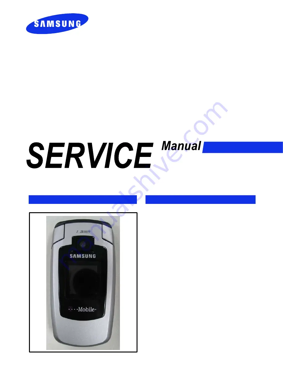
background image

GSM TELEPHONE

SGH-T619

GSM TELEPHONE

CONTENTS

1.

Safety Precautions

2.

Specification

3.

Product Function

4.

Array course control

5.

Exploded View/Disassembly

and Assembly Instructions

6.

MAIN Electrical Parts List

7.

Block Diagrams

8.

PCB Diagrams

9.

Flow Chart of Troubleshooting

10. Reference data

Summary of Contents for SGH-T619

Page 1: ...S 1 Safety Precautions 2 Specification 3 Product Function 4 Array course control 5 Exploded View Disassembly and Assembly Instructions 6 MAIN Electrical Parts List 7 Block Diagrams 8 PCB Diagrams 9 Flow Chart of Troubleshooting 10 Reference data ...

Page 2: ...tronics Co Ltd Code No GH68 12345A 2006 08 Rev 1 0 ⓒ This Service Manual is a property of Samsung Electronics Co Ltd Any unauthorized use of Manual can be punished under applicable International and or domestic law ...

Page 3: ...1 Downloading Binary Files 4 2 4 2 Pre requsite for Downloading 4 2 4 3 S W Downloader Program 4 3 5 Exploded View Disassembly Assembly Instructions 5 1 Cellular phone Exploded View 5 1 5 2 Cellular phone Parts list 5 2 5 3 Disassembly Assembly Instructions 5 4 6 MAIN Electrical Parts List 7 Block Diagrams 7 1 RF Solution Block Diagram 7 1 7 2 Base Band Solution Block Diagram 7 2 7 3 Audio Block 7...

Page 4: ...Part 9 10 9 7 Key Data Input 9 12 9 8 Receiver Part 9 14 9 9 Back Light 9 16 9 10 Key Back Light 9 18 9 11 Camera Part 9 20 9 12 GSM850 Reciever 9 23 9 13 GSM850 Transmitter 9 24 9 14 GSM900 Reciever 9 25 9 15 GSM900 Transmitter 9 26 9 16 DCS Receiver 9 27 9 17 DCS Transmitter 9 28 9 18 PCS Receiver 9 29 9 19 PCS Transmitter 9 30 10 Reference data ...

Page 5: ...orn away Use a thicken twisted wire when you measure level A thicken twisted wire has low resistance therefore error of measurement is few Repair after separate Test Pack and Set because for short danger for example an overcurrent and furious flames of parts etc when you repair board in condition of connecting Test Pack and tuning on Take specially care of soldering because Land of PCB is small an...

Page 6: ...ined your body before you touch semiconductor or parts with semiconductor There are ways that you touch an earthed place or wear static electricity prevention string on wrist Use earthed soldering steel when you connect or disconnect ESD Use soldering removing tool to break static electricity otherwise ESD will be damaged by static electricity Don t unpack until you set up ESD on product Because m...

Page 7: ... 975 1023 512 885 512 810 Tx Rx spacing 45MHz 45MHz 45MHz 95MHz 80MHz Mod Bit rate Bit Period 270 833kbps 3 692us 270 833kbps 3 692us 270 833kbps 3 692us 270 833kbps 3 692us 270 833kbps 3 692us Time Slot Period Frame Period 576 9us 4 615ms 576 9us 4 615ms 576 9us 4 615ms 576 9us 4 615ms 576 9us 4 615ms Modulation 0 3GMSK 0 3GMSK 0 3GMSK 0 3GMSK 0 3GMSK MS Power 33dBm 13dBm 33dBm 13dBm 33dBm 5dBm 3...

Page 8: ... DCS1800 0 30 3 dBm 1 28 3 dBm 2 26 3 dBm 3 24 3 dBm 4 22 3 dBm 5 20 3 dBm 6 18 3 dBm 7 16 3 dBm 8 14 3 dBm 9 12 4 dBm 10 10 4 dBm 11 8 4dBm 12 6 4 dBm 13 4 4 dBm 14 2 5 dBm 15 0 5 dBm TX Power control level GSM900 5 33 3 dBm 6 31 3 dBm 7 29 3 dBm 8 27 3 dBm 9 25 3 dBm 10 23 3 dBm 11 21 3 dBm 12 19 3 dBm 13 17 3 dBm 14 15 3 dBm 15 13 3 dBm 16 11 5 dBm 17 9 5 dBm 18 7 5 dBm 19 5 5 dBm TX Power cont...

Page 9: ...duct Function 3 1 This Document can not be used without Samsung s authorization Main Function 1 3M Camera and camcorder MP3 player MP3 AAC AAC Phonebook Name card Multimedia Message Service MMS E mail Voice recorder Bluetooth USB SyncML Web browser Java Calendar ...

Page 10: ...SAMSUNG Proprietary Contents may change without notice Product Function 3 2 This Document can not be used without Samsung s authorization ...

Page 11: ...G Proprietary Contents may change without notice 4 Array course control 4 1 This Document can not be used without Samsung s authorization Test Jig GH80 03307A Test Cable GH39 00337A RF Test Cable GH39 00283A ...

Page 12: ...tion Software Downloading 4 1 Downloading Binary Files Swift Model firmware is composed of 3 files cla Main source binary tfs File which includes image mp3 etc which are needed for each application cfg File which has information about tfs File 4 2 Pre requsite for Downloading Downloader Single or Multi downloader The firmware Data Cable ...

Page 13: ...may change without notice Array course control 4 3 This Document can not be used without Samsung s authorization 4 3 S W Downloader Program 1 Unzip the downloader and firmware files to a folder where you want 2 Open the downloader ...

Page 14: ...SAMSUNG Proprietary Contents may change without notice Array course control 4 4 This Document can not be used without Samsung s authorization 3 Set the serial Port and BAUD rate ...

Page 15: ...SAMSUNG Proprietary Contents may change without notice Array course control 4 5 This Document can not be used without Samsung s authorization 4 Check radio button Binary only TFS Only and Binary TFS ...

Page 16: ...SAMSUNG Proprietary Contents may change without notice Array course control 4 6 This Document can not be used without Samsung s authorization 5 Select the binary and TFS file s that you want to download ...

Page 17: ...SAMSUNG Proprietary Contents may change without notice Array course control 4 7 This Document can not be used without Samsung s authorization 6 Press start button and power on the phone ...

Page 18: ...UNG Proprietary Contents may change without notice Array course control 4 8 This Document can not be used without Samsung s authorization then the downloader can recognize the flash memory type of the phone ...

Page 19: ...SAMSUNG Proprietary Contents may change without notice Array course control 4 9 This Document can not be used without Samsung s authorization 7 After confirming the memory type press DOWNLOAD button ...

Page 20: ...SAMSUNG Proprietary Contents may change without notice Array course control 4 10 This Document can not be used without Samsung s authorization ...

Page 21: ...Samsung s authorization 5 Exploded View Disassembly Assembly Instructions 5 1 Cellular phone Exploded View QWD02 QCK01 QFR01 QME01 QMP01 QMI03 QCR31 QAN05 QAN02 QRE01 QCR31 QBA01 QBA00 QVO01 QRF03 QSP01 QCR47 QCW01 QLC01 QMW02 QMW01 QCA01 QHI01 QFL01 QCR31 QSC11 QSC12 QMO01 QFU02 QFU01 QKP01 QIF01 ...

Page 22: ...8 01923A QME01 UNIT METAL DOME GH59 03271A QMI03 RMO CUSHION RUBBER MIC GH73 07303A QMO01 MOTOR DC SPHM500 GH31 00242A QMP01 PBA MAIN SGHT619 GH92 02973A QSC11 MPR SHEET FOLDER SCREW CAP R GH74 21404A QSC12 MPR SHEET FOLDER SCREW CAP L GH74 23942A QSP01 SPEAKER 3001 002041 QWD02 PCT SUB WINDOW GH72 30894A QFL01 ASSY CASE FOLDER LOWER GH98 01036A QHI01 ASSY MEC HINGE CAN TYPE GH75 04662A QRE01 ASSY...

Page 23: ... GAKSET LCD GH74 25156A MPR GASK TAPE GH74 25157A MPR GASKET TAPE GH74 26789A MPR GASK TAPE FRONT GH74 26852A MPR REMOVE TAPE LCD GH74 13804A MPR TAPE LED GH74 17926A MPR TAPE REMOVE LCD GH74 18286A MPR TAPE SUB LCD INSUL GH74 18531A MPR TAPE MAIN LDI GH74 19992A MPR VINYL BOHO MAIN WINDOW GH74 22341A MPR TAPE 28X7XT0 05 TESA4965 GH74 26546A MPR TAPE 24 3X3XT0 05 TESA4965 GH74 26547A MPR CUSHION S...

Page 24: ... may not go to REAR 1 Take care so that damage may not occur to LCD CONNECTOR FPCB 1 Take care so that damage may not occur to SPEAKER FPCB LCD and CAMERA CONNECTOR FPCB 2 Take care lest BGA parts breakdown should occur 1 Removed RF COVER in the left side top portion 2 Open earphone COVER I F COVER 1 1 Disjoint the 4 screws of rear plastic 2 Disjoint set from lower part 2 3 1 Separate the LCD CONN...

Page 25: ...breakdown should occur 1 When separate observe in FRONT warp 2 Take care of be tearing LCD and CAMERA FPCB 3 Be careful of the damage of appearance and scratch 1 Remove using tweezers 2 Be careful of the damage of appearance and scratch 1 Be careful of the damage of appearance and scratch 5 6 7 8 1 Remove dust prevention TAPE 1 Separate FRONT from FOLDER by pressing FOLDER hinge 1 Remove SCREW COV...

Page 26: ...en separate take care lest wire should be cut 2 Be careful of the damage of appearance and scratch 1 Be careful of the damage of appearance and scratch 2 Pay attention to F PCB damage 1 Be careful of the damage of appearance and scratch 9 10 11 12 1 Disjoint from lower part using decomposition beam 2 Pick out F PCB 1 Using tweezers separate speaker from FOLDER LOWER 1 Separate F PCB by opening CAM...

Page 27: ...t can not be used without Samsung s authorization 1 Be careful of the damage of appearance and scratch 2 Pay attention to CAMERA FPCB damage 1 Be careful of the damage of appearance and scratch 13 1 Separate CAMERA module from FOLDER LOWER by using tweezers 1 After disjointing INTENNA SCREW separate INTENNA from REAR 15 ...

Page 28: ...and scratch 2 Pay attention to F PCB damage 1 Be careful of the damage of appearance and scratch 1 2 3 4 1 Joint INTENNA to REAR by SCREW 1 Combine camera and LCD MODULE 2 Insert CAMERA module to FOLDER LOWER 3 Preserve CAMERA CONNECTOR not to come out set LCD safely on LOWER 1 Install LCD module to UPPER 2 Install SPEAKER preserving WIRE threads not to get snarl 3 Attach CAMERA CONNECTOR fixing i...

Page 29: ...g s authorization 1 Be careful of the damage of appearance and scratch 2 When pass home observe as F PCB does not damage 1 Confirm whether KEYPAD matches rear exactly when KEYPAD be set 7 8 1 Pass LCD module F PCB through REAR s aperture 2 By pressing hinge combine FOLDER and FRONT 1 Set KEYPAD safely to FRONT 7 8 1 Joint 2 SCREWs 1 Attach SCREW COVER ...

Page 30: ...ntion to F PCB damage 1 Assemble by observing on LCD CONNECTOR direction 2 Confirm whether click sound sounds when contract 1 Be careful of the damage of appearance and scratch 1 Be careful of the damage of appearance and scratch 10 9 1 Set BOARD safely to REAR 2 Combine LCD CONNECTOR 1 Attach dust protection TAPE 11 12 1 Combine FRONT and REAR from upper direction 1 Joint SCREW ...

Page 31: ... Exploded View Disassembly Assembly Instructions 5 11 This Document can not be used without Samsung s authorization 1 Be careful of the damage of appearance and scratch 13 1 Attach RF COVER in the left side top portion 2 Insert earphone COVER and I F COVER ...

Page 32: ...SAMSUNG Proprietary Contents may change without notice Exploded View Disassembly Assembly Instructions 5 12 This Document can not be used without Samsung s authorization ...

Page 33: ...03 000812 SA C120 C CER CHIP 2203 001383 SA C121 C CER CHIP 2203 000254 SA C122 C CER CHIP 2203 000812 SA C125 C CER CHIP 2203 005450 SA C127 C CER CHIP 2203 006190 SA C128 C CER CHIP 2203 006642 SA C129 C CER CHIP 2203 005736 SA C130 C CER CHIP 2203 000812 SA C131 C CER CHIP 2203 005053 SA C132 C CER CHIP 2203 005054 SA C134 C CER CHIP 2203 005446 SA C135 C CER CHIP 2203 000438 SA C136 C CER CHIP...

Page 34: ...CER CHIP 2203 000386 SA C408 C CER CHIP 2203 000386 SA C411 C CER CHIP 2203 000812 SA C412 C CER CHIP 2203 006208 SA C414 C CER CHIP 2203 006208 SA C415 C CER CHIP 2203 006257 SA C416 C CER CHIP 2203 006257 SA C418 C CER CHIP 2203 006208 SA C419 C CER CHIP 2203 005482 SA C422 C CER CHIP 2203 006208 SA C423 C CER CHIP 2203 006208 SA C424 C CER CHIP 2203 006257 SA C425 C CER CHIP 2203 006257 SA C426...

Page 35: ...203 006361 SA C703 C CER CHIP 2203 006190 SA C704 C CER CHIP 2203 006048 SA C705 C CER CHIP 2203 005682 SA C706 C CER CHIP 2203 005682 SA C707 C CER CHIP 2203 005682 SA C708 C CER CHIP 2203 005682 SA C709 C CER CHIP 2203 005682 SA C710 C CER CHIP 2203 005682 SA C711 C CER CHIP 2203 005682 SA C712 C CER CHIP 2203 005682 SA C713 C CER CHIP 2203 005682 SA C714 C CER CHIP 2203 005682 SA C715 C CER CHI...

Page 36: ...41 INDUCTOR SMD 2703 002201 SA L201 BEAD SMD 3301 001729 SA L500 INDUCTOR SMD 2703 002962 SA L601 INDUCTOR SMD 2703 002204 SA L603 INDUCTOR SMD 2703 002204 SA L617 INDUCTOR SMD 2703 002204 SA L618 INDUCTOR SMD 2703 002204 SA L701 BEAD SMD 3301 001534 SA LED700 LED 0601 002094 SA LED701 LED 0601 002094 SA LED702 LED 0601 002094 SA LED703 LED 0601 002094 SA LED704 LED 0601 002094 SA LED705 LED 0601 ...

Page 37: ...HIP 2007 000171 SA R311 R CHIP 2007 000171 SA R314 R CHIP 2007 000171 SA R315 R CHIP 2007 000162 SA R401 R CHIP 2007 007100 SA R402 R CHIP 2007 000171 SA R403 R CHIP 2007 000171 SA R404 R CHIP 2007 008055 SA R405 R CHIP 2007 002796 SA R500 R CHIP 2007 000162 SA R501 R CHIP 2007 000758 SA R502 R CHIP 2007 000758 SA R503 R CHIP 2007 008516 SA R504 R CHIP 2007 007334 SA R506 R CHIP 2007 009084 SA R50...

Page 38: ...SA R711 R CHIP 2007 000171 SA R712 R CHIP 2007 000171 SA R713 R CHIP 2007 009157 SA R714 R CHIP 2007 001298 SA R715 R CHIP 2007 001298 SA RFS100 CONNECTOR COAXIAL 3705 001421 SA SIM400 CONNECTOR CARD EDGE 3709 001400 SA TA123 C TA CHIP 2404 001411 SA TA400 C TA CHIP 2404 001381 SA TA504 C TA CHIP 2404 001268 SA TA507 C TA CHIP 2404 001380 SA TA600 C TA CHIP 2404 001281 SA TA622 C TA CHIP 2404 0012...

Page 39: ...3 SA VR400 VARISTOR 1405 001082 SA VR500 THERMISTOR NTC 1404 001221 SA VR600 VARISTOR 1405 001138 SA VR601 VARISTOR 1405 001138 SA VR700 VARISTOR 1405 001082 SA VR701 VARISTOR 1405 001138 SA VR702 VARISTOR 1405 001138 SA VR703 VARISTOR 1405 001138 SA VR704 VARISTOR 1405 001138 SA VR705 VARISTOR 1405 001138 SA ZD500 DIODE TVS 0406 001188 SA ZD505 DIODE ZENER 0403 001427 SA ZD506 DIODE ZENER 0403 00...

Page 40: ...SAMSUNG Proprietary Contents may change without notice Main Electrical Parts List 6 8 This Document can not be used without Samsung s authorization ...

Page 41: ...SAMSUNG Proprietary Contents may change without notice This Document can not be used without Samsung s authorization 7 Block Diagrams 7 1 7 1 RF Solution Block Diagram ...

Page 42: ...SAMSUNG Proprietary Contents may change without notice Block Diagrams This Document can not be used without Samsung s authorization 7 2 7 2 Base Band Solution Block Diagram ...

Page 43: ...SAMSUNG Proprietary Contents may change without notice Block Diagrams This Document can not be used without Samsung s authorization 7 3 7 3 AUDIO BLOCK ...

Page 44: ...SAMSUNG Proprietary Contents may change without notice Block Diagrams This Document can not be used without Samsung s authorization 7 4 7 4 CAMERA BLOCK ...

Page 45: ...SAMSUNG Proprietary Contents may change without notice 8 PCB Diagrams 8 1 This Document can not be used without Samsung s authorization 8 1 MAIN Top ...

Page 46: ...SAMSUNG Proprietary Contents may change without notice PCB Diagrams 8 2 This Document can not be used without Samsung s authorization Bottom ...

Page 47: ...r On does not work Charge the Battery END No Yes C406 VINT 2 7V Check the PMU related to VINT No Yes Check the Clock at R401 32KHZ Resolder OSC400 No Yes C425 VDD_IO_LOW C424 VDD_IO_HIGH H Check the related circuit No Yes TA507 VDD_GSM_CORE 1 875V Check the VDD_GSM_CORE circuit No Yes Check for the clock at C114 26MHz Check the clock generation circuit related to OSC100 No Yes Check the initial op...

Page 48: ...SAMSUNG Proprietary Contents may change without notice This Document can not be used without Samsung s authorization Flow Chart of Troubleshooting 9 2 ...

Page 49: ...hart of Troubleshooting This Document can not be used without Samsung s authorization 9 3 9 2 Initial TP224 RSTON H Initial Failure Check the circuit related to reset END No Yes Is U308 pin 4 OK Yes Yes No Check the U305 Check the 16bit data signal memory CE Yes ...

Page 50: ...SAMSUNG Proprietary Contents may change without notice This Document can not be used without Samsung s authorization Flow Chart of Troubleshooting 9 4 ...

Page 51: ...t Samsung s authorization 9 5 9 3 Charging Part Check the U501 pin 16 4 9V Abnormal charging part END No Yes U501 pin 12 L No Yes U501 pin 4 L No Yes Check the U501 pin 15 4 2V No Yes Check the circuit related to V_EXT_CHARGE Resolder or replace U501 Check the circuit related to AUX_ON signal Resolder or replace U501 Yes ...

Page 52: ...ion Flow Chart of Troubleshooting 9 6 9 4 Sim Part SIM400 pin 1 5 H Phone can t access SIM Card Check the sim charge pump Check the SIM Card END No Yes Yes Yes No Check the Clock After Power ON Check SIMCLK Signal on pin3 of SIM400 in a few second Yes No Replace PBA After SIM card insert SIM400 pin 2 H SIM_RST Yes ...

Page 53: ...SAMSUNG Proprietary Contents may change without notice Flow Chart of Troubleshooting This Document can not be used without Samsung s authorization 9 7 ...

Page 54: ... Chart of Troubleshooting 9 8 9 5 Microphone Part Check the connection status of MIC MIC600 Check the inductors L601 L603 Re Solder the Mic MIC600 Resolder the L601 and L603 END No Yes Yes Yes Yes No Check MIC_BIAS H No Resolder R616 R600 TA600 R604 R605 Microphone does not work Check the MIC No Replace the microphone Yes ...

Page 55: ...SAMSUNG Proprietary Contents may change without notice Flow Chart of Troubleshooting This Document can not be used without Samsung s authorization 9 9 ...

Page 56: ...g 9 10 9 6 Speaker Part Speaker does not work Check the supply voltage of U601 Is the TA632 3 8V Check the VBAT or replace TA632 No Yes Is the D Amp U601 output working Check R621 and R622 Resolder R621 R622 or replace U601 No Yes END Is Speaker working Change the Speaker No Yes Yes Check the connection status of SPK Re solder the Speaker No Yes ...

Page 57: ...SAMSUNG Proprietary Contents may change without notice Flow Chart of Troubleshooting This Document can not be used without Samsung s authorization 9 11 ...

Page 58: ...without Samsung s authorization Flow Chart of Troubleshooting 9 12 9 7 Key Data Input When any key input is given is there something on LCD display Check the Dome sheet Key Pad END No Yes Yes Check Initial Operation When one of the keys is pushed KBIO signal is OK Replace the PBA No Yes ...

Page 59: ...SAMSUNG Proprietary Contents may change without notice Flow Chart of Troubleshooting This Document can not be used without Samsung s authorization 9 13 ...

Page 60: ...rt of Troubleshooting 9 14 9 8 Receiver Part Check the power of analog switch U600 Is R623 3 8V Resolder R623 END No Yes Yes Receiver does not work Check the AUDIO_SEL Pin of U600 Is Pin 2 L Check UCP200 No Yes Is Receiver working Replace the Receiver No Yes Check the connection status of Receiver No Resolder the receiver Yes ...

Page 61: ...SAMSUNG Proprietary Contents may change without notice Flow Chart of Troubleshooting This Document can not be used without Samsung s authorization 9 15 ...

Page 62: ...Chart of Troubleshooting 9 16 9 9 Back Light for LCD Is LCD Contrast set on high level in the Menu Set LCD Contrast on high level END No Yes Yes Backlight does not work HDC700 Pin43 H Check the UCP200 No Yes Check the VBAT pins of HDC700 Pin 38 40 42 3 8V Check the related circuit of VBAT No Yes Yes Replace the LCD Module ...

Page 63: ...SAMSUNG Proprietary Contents may change without notice Flow Chart of Troubleshooting This Document can not be used without Samsung s authorization 9 17 ...

Page 64: ...ice This Document can not be used without Samsung s authorization Flow Chart of Troubleshooting 9 18 9 10 Key Back Light U700 pin 6 H Check the U700 related to KEY_LED_ON signal END No Yes Yes Main Key LED does not work U700 pin 3 H No Replace U700 Yes ...

Page 65: ...SAMSUNG Proprietary Contents may change without notice Flow Chart of Troubleshooting This Document can not be used without Samsung s authorization 9 19 ...

Page 66: ...ra part Camera function does not work Yes No Reconnect the camera module Check the Camera connector status CN103 Yes HDC700 pin 44 1 5V No Check the LDO U314 related with VDD_CAM_1V5 Yes R308 26MHz No Check the related to 27MHz clock U303 Yes Is there another problem END Replace the camera module Yes HDC700 pin 46 2 8V No Resolder C422 or check the PMU U400 Yes ...

Page 67: ...SAMSUNG Proprietary Contents may change without notice Flow Chart of Troubleshooting This Document can not be used without Samsung s authorization 9 21 ...

Page 68: ...SAMSUNG Proprietary Contents may change without notice This Document can not be used without Samsung s authorization Flow Chart of Troubleshooting 9 22 ...

Page 69: ...r freq 67 7kHz Amp 50dBm Yes F101 Pin10 65dBm No Resolder RFS100 C101 L141 Yes Check F101 pin13 15 16 L pin11 H Check ANT Switch control circuit F101 pin6 7 68dBm No No Resolder F101 Yes Yes Resolder C104 C105 L103 U102 pin 29 74dBm pin 30 74dBm No Yes Check Resolder U102 R138 C114 RF26MHz RF PSU Part No Check U102 pin 23 26 31 2 7V No U102 pin 7 8 9 10 1V Resolder U102 Yes Yes Check UCP200 END ...

Page 70: ...2 pin38 15dBm PAM100 pin9 11dBm Check ANT Switch control circuit Change or Resolder F101 Resolder C131 L111 C141 Yes Check VBAT or PAM control signal No No No No No No Yes Yes Yes Yes Yes Yes Check F101 pin13 H 2 68V pin11 15 16 L Check PAM100 pin 3 4 5 6 7 OK Yes Resolder or Change PAM100 Resolder U102 No U102 pin 6 7 8 9 1V Check Resolder RFLO signal RF26MHz RF PSU Part No Yes Yes END Check UCP2...

Page 71: ...nter freq 67 7kHz Amp 50dBm Yes F101 Pin10 65dBm No Resolder RFS100 C101 L141 Yes Check ANT Switch control circuit F101 pin6 7 68dBm Check F101 pin11 13 15 16 L No No Resolder F101 Yes Yes Resolder C104 C105 L103 U102 pin 29 74dBm pin 30 74dBm No Yes Check Resolder U102 R138 C114 RF26MHz RF PSU Part No Check U102 pin 23 26 31 2 7V No U102 pin 7 8 9 10 1V Resolder U102 Yes Yes Check UCP200 END ...

Page 72: ...2 pin38 15dBm PAM100 pin9 11dBm Check ANT Switch control circuit Change or Resolder F101 Resolder C131 L111 C141 Yes Check VBAT or PAM control signal No No No No No No Yes Yes Yes Yes Yes Yes Check F101 pin13 H 2 68V pin11 15 16 L Check PAM100 pin 3 4 5 6 7 OK Yes Resolder or Change PAM100 Resolder U102 No U102 pin 6 7 8 9 1V Check Resolder RFLO signal RF26MHz RF PSU Part No Yes Yes END Check UCP2...

Page 73: ...er freq 67 7kHz Amp 50dBm Yes F101 Pin10 65dBm No Resolder RFS100 C101 L141 Yes Check ANT Switch control circuit F101 pin1 2 68dBm Check F101 pin11 13 15 16 L No No Resolder F101 Yes Yes Resolder C120 L109 L115 U102 pin 35 74dBm pin 36 74dBm No Yes Check Resolder U102 R138 C114 RF26MHz RF PSU Part No Check U102 pin 23 26 31 2 7V No U102 pin 7 8 9 10 1V Resolder U102 Yes Yes Check UCP200 END ...

Page 74: ... Yes No No No No No No No No Check Resolder RFLO signal RF26MHz RF PSU Part Check VBAT or PAM control signal Resolder or Change PAM100 Check PAM100 pin 3 4 5 6 7 OK Yes U102 pin 6 7 8 9 1V Resolder C107 L101 C108 L104 C109 Resolder C125 L110 C140 Change or Resolder F101 Check ANT Switch control circuit PAM100 pin1 11dBm U102 pin2 15dBm PAM100 pin14 18dBm F101 pin14 18dBm Check F101 pin15 16 H 2 68...

Page 75: ... freq 67 7kHz Amp 50dBm Yes Resolder RFS100 C101 L141 No F101 Pin10 65dBm Yes Check F101 pin15 H pin11 13 16 L F101 pin3 4 68dBm Check ANT Switch control circuit No No Yes Resolder F101 Yes Resolder C113 C119 L108 U102 pin 32 74dBm pin 33 74dBm No Yes Check Resolder U102 R138 C114 RF26MHz RF PSU Part Check U102 pin 23 26 31 2 7V No U102 pin 7 8 9 10 1V No Resolder U102 Yes Yes Check UCP200 END ...

Page 76: ... Yes No No No No No No No No Check Resolder RFLO signal RF26MHz RF PSU Part Check VBAT or PAM control signal Resolder or Change PAM100 Check PAM100 pin 3 4 5 6 7 OK Yes U102 pin 6 7 8 9 1V Resolder C107 L101 C108 L104 C109 Resolder C125 L110 C140 Change or Resolder F101 Check ANT Switch control circuit PAM100 pin1 11dBm U102 pin2 15dBm PAM100 pin14 18dBm F101 pin14 18dBm Check F101 pin15 16 H 2 68...

Page 77: ...SAMSUNG Proprietary Contents may change without notice Flow Chart of Troubleshooting This Document can not be used without Samsung s authorization 9 31 ...

Page 78: ...SAMSUNG Proprietary Contents may change without notice This Document can not be used without Samsung s authorization Flow Chart of Troubleshooting 9 32 ...

Page 79: ... EEPROM Electrically Erasable Programmable Read Only Memory EGPRS Enhanced GPRS ETM Embedded Trace Macrocell ETSI European Telecommunications Standards Institute FM Frequency Modulation FPGA Field Programmable Gate Array FR Full Rate FTA Full Type Approval GSM specification GPIO General Purpose Input Output GPRS General Packet Radio Service GSM Global System for Mobile communication I2C Inter IC C...

Page 80: ...Code Modulation PDCU Power Down Control Unit PIO Parallel IO unit PLL Phase Locked Loop RAM Random Access Memory ROM Read Only Memory SRAM Static Random Access Memory SW Software TDMA Time Division Multiple Access UART Universal Asynchronous Receiver Transmitter UMTS Universal Mobile Telecommunication System USB Universal Serial Bus USIM UMTS SIM ...

Reviews: