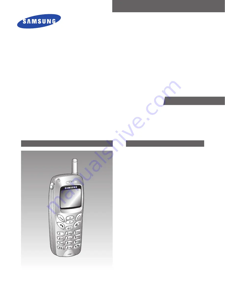
background image

ELECTRONICS

SERVICE

DUAL BAND Mobile
Cellular Phone 

SGH-R210E

Manual

DUAL BAND MOBILE CELLULAR PHONE

CONTENTS

1. Exploded Views and Parts List

2. PCB Diagrams

3. Electrical Parts List

4. Block Diagrams

5. Flow Chart of Troubleshooting and

Circuit Diagrams

Summary of Contents for SGH-R210E

Page 1: ... BAND Mobile Cellular Phone SGH R210E Manual DUAL BAND MOBILE CELLULAR PHONE CONTENTS 1 Exploded Views and Parts List 2 PCB Diagrams 3 Electrical Parts List 4 Block Diagrams 5 Flow Chart of Troubleshooting and Circuit Diagrams ...

Page 2: ...Samsung Electronics Co Ltd Printed in Korea 05 2002 Rev 1 0 GH68 02809A ELECTRONICS ...

Page 3: ...ain Bottom 3 Electrical Parts List 3 1 Main Parts List Top 3 2 Main Parts List Bottom 4 Block Diagrams 4 1 Main Baseband 4 2 Main RF 4 2 1 RF Transmit Part 4 2 2 RF Receive Part 5 Flow Chart of Troubleshooting and Circuit Diagrams 5 1 Power ON 5 2 Initial 5 3 Charging Part 5 4 Sim Part 5 5 Microphone Part 5 6 Speaker Part 5 7 Key Data Input 5 8 Alert Tone 5 9 Ring Indicator 5 10 Back Light 5 11 GS...

Page 4: ...Exploded Views and Parts List 1 1 1 SGH R210E Exploded Views and Parts List 1 1 Main 1 4 5 7 2 7 1 7 8 10 12 13 2 3 6 14 9 11 ...

Page 5: ...84A GH75 01160A 3002 001098 GH92 01315A GH07 00075B GH72 02984B GH73 00758C GH31 00019A GH42 00120A GH75 01165C GH73 00759C 6001 001542 GH43 00369C GH75 01484B 3001 001233 GH59 00240B GH72 02784A GH75 01160A 3002 001098 GH92 01315A GH07 00075B GH72 02984B GH73 00758B GH31 00019A GH42 00120B GH75 01165B GH73 00759B 6001 001542 GH43 00369B GH75 01484A 3001 001233 GH59 00240B GH72 02784A GH75 01160A ...

Page 6: ...Exploded Views and Parts List 1 3 1 4 Travel Adapter Parts List TYPE SEC CODE REMARK A GH44 00171A CHINA B GH44 00184A EUROPE C GH44 00171C UNITED KINGDOM D Gh44 00171E TAIWAN 1 3 Travel Adapter A B C D ...

Page 7: ...1 4 1 5 Ciger Light Adapter Exploded Views and Parts List 1 6 Ciger Light Adapter Parts List DESCRIPTION SEC CODE REMARK Ciger Light Adapter Code GH44 00170A BLACK ...

Page 8: ...1 5 Exploded Views and Parts List 1 7 Test Jig TEST JIG GH80 10508A TEST JIG CABLE GH39 00079A RF CABLE GH39 00090A ...

Page 9: ...1 6 Exploded Views and Parts List 1 7 1 Test Jig DC POWER SUPPLY 232 CABLE TEST JIG CABLE RF CABLE 8922 or 8960 WIRELESS COMMUNICATIONS TEST SET Note PC ...

Page 10: ...Exploded Views and Parts List 1 7 1 8 EAR Microphone EAR MICROPHONE GH59 00225B 1 9 Data Kit DATA KIT GH39 00078A 1 10 Battery Charger BATTERY CHAGER GH44 00234A ...

Page 11: ...PCB Diagrams 2 1 2 PCB Diagrams 2 1 Main Top ...

Page 12: ...PCB Diagrams 2 2 2 2 Main Bottom ...

Page 13: ...TE85L 17 U465 0504 001058 TR DIGITAL RN4985 NPN PNP 200mW 2 2Kohm 47Kohm RN4985 TE85L 18 U492 0504 001058 TR DIGITAL RN4985 NPN PNP 200mW 2 2Kohm 47Kohm RN4985 TE85L 19 Q401 0505 001332 FET SILICON FDG6301 N 25V 0 22A 4OHM 3W SC70 6 FDG6301N 20 U474 0505 001376 FET SILICON FDC6329L N P 8V 2 5A 0 7W SC 74 SI3865DV T1 21 Q402 0505 001570 FET SILICON N P 0 4W SC70 6 SI1865DL T1 22 U309 0506 001004 TR...

Page 14: ...R444 2007 000139 R CHIP 220ohm 5 1 16W DA TP 1005 ERJ2GEJ221X 52 R447 2007 000139 R CHIP 220ohm 5 1 16W DA TP 1005 ERJ2GEJ221X 53 R106 2007 000140 R CHIP 1Kohm 5 1 16W DA TP 1005 MCR01MZSJ102 54 R575 2007 000140 R CHIP 1Kohm 5 1 16W DA TP 1005 MCR01MZSJ102 55 R584 2007 000140 R CHIP 1Kohm 5 1 16W DA TP 1005 MCR01MZSJ102 56 R738 2007 000140 R CHIP 1Kohm 5 1 16W DA TP 1005 MCR01MZSJ102 57 R103 2007 ...

Page 15: ...16W DA TP 1005 ERJ2GEJ104X 94 R606 2007 000162 R CHIP 100Kohm 5 1 16W DA TP 1005 ERJ2GEJ104X 95 R638 2007 000162 R CHIP 100Kohm 5 1 16W DA TP 1005 ERJ2GEJ104X 96 R440 2007 000168 R CHIP 470Kohm 5 1 16W DA TP 1005 RK73K1ETP474J 97 R577 2007 000172 R CHIP 10ohm 5 1 16W DA TP 1005 RC1005J100CS 98 R578 2007 000172 R CHIP 10ohm 5 1 16W DA TP 1005 RC1005J100CS 99 R105 2007 001244 R CHIP 91Kohm 5 1 16W D...

Page 16: ...P 1005 GRP1555C1H101JD01E 138 C718 2203 000233 C CERAMIC CHIP 0 1nF 5 50V NP0 TP 1005 GRP1555C1H101JD01E 139 C764 2203 000233 C CERAMIC CHIP 0 1nF 5 50V NP0 TP 1005 GRP1555C1H101JD01E 140 C789 2203 000233 C CERAMIC CHIP 0 1nF 5 50V NP0 TP 1005 GRP1555C1H101JD01E 141 C791 2203 000233 C CERAMIC CHIP 0 1nF 5 50V NP0 TP 1005 GRP1555C1H101JD01E 142 C792 2203 000233 C CERAMIC CHIP 0 1nF 5 50V NP0 TP 100...

Page 17: ...P0 TP 1005 CM05CG270J50AH 181 U690 2203 000679 C CERAMIC CHIP 0 027nF 5 50V NP0 TP 1005 CM05CG270J50AH 182 C143 2203 000812 C CERAMIC CHIP 0 033nF 5 50V NP0 TP 1005 GRP1555C1H330JZ01E C01 183 C264 2203 000812 C CERAMIC CHIP 0 033nF 5 50V NP0 TP 1005 GRP1555C1H330JZ01E C01 184 C310 2203 000812 C CERAMIC CHIP 0 033nF 5 50V NP0 TP 1005 GRP1555C1H330JZ01E C01 185 C311 2203 000812 C CERAMIC CHIP 0 033n...

Page 18: ...7 2203 005061 C CERAMIC CHIP 100nF 80 20 16V Y5V TP 1005 GRP155F51C104ZA01E 223 C701 2203 005061 C CERAMIC CHIP 100nF 80 20 16V Y5V TP 1005 GRP155F51C104ZA01E 224 C706 2203 005061 C CERAMIC CHIP 100nF 80 20 16V Y5V TP 1005 GRP155F51C104ZA01E 225 C711 2203 005061 C CERAMIC CHIP 100nF 80 20 16V Y5V TP 1005 GRP155F51C104ZA01E 226 C318 2203 005065 C CERAMIC CHIP 1000nF 80 20 10V Y5V TP 1608 CL10F105ZP...

Page 19: ...03 002269 INDUCTOR SMD 56NH 10 1 0X0 5X0 5MM CIH05T56NJNC 263 L612 2703 002416 INDUCTOR SMD 3 9NH 5 1608 0603CS 3N9XJBW 264 X1 2801 004060 CRYSTAL SMD 0 032768MHZ 30PPM 12 5PF MS2V TS 90OHM TR 265 U100 2809 001254 OSCILLATOR VCTCXO 13MHZ 3PPM 10KOHM 10PF TOA1300VAI4KRA TP 3V 2MA 266 F205 2904 001386 FILTER SAW 942 5MHZ 1 9DB TP B7706 925 960MHZ 2 6DB 267 F204 2904 001387 FILTER SAW 1 8425GHZ 1 1DB...

Page 20: ...art Description Vendor Part No ence CODE 281 GH72 02984B PPR SGHR210 SGH R210 PET SUS301 WHT SGHR210 METAL DOME METAL DOME 51 38X39 52 282 GH74 02030A MPR ANT CONTACT SGH R210 PORON SPONGE SGH R210 ANT SPONGE 5X4XT0 7 BLK CONTACT SPON 3 8 ...

Page 21: ...01094 LED CHIP Y GRN 0 8x1 1mm 570nm SSCYG101TS 19 D448 0601 001094 LED CHIP Y GRN 0 8x1 1mm 570nm SSCYG101TS 20 D449 0601 001094 LED CHIP Y GRN 0 8x1 1mm 570nm SSCYG101TS 21 D450 0601 001094 LED CHIP Y GRN 0 8x1 1mm 570nm SSCYG101TS 22 D451 0601 001094 LED CHIP Y GRN 0 8x1 1mm 570nm SSCYG101TS 23 LED1 0601 001402 LED CHIP RED Y GRN 1 2x1 5mm 660 570nm CL 165HR YG D 24 LED2 0601 001540 LED CHIP BL...

Page 22: ...y Temperature 3VAERO RTC_3V3 Serial Data Interface I O Interface A D Interface AFC PLL LOAD SWITCH Charging Circuit Li Ion Battery Standard ONE C VIBRATOR SYSTEM CLOCK 13MHz SRAM FLASH EEPROM RTC_CLOCK 32 768KHz KEYPAD SIM CARD SPEAKER MIC LCD BB INTERFACE RF INTERFACE LVCC AVCC VDD3 0 3VRF ...

Page 23: ... Filter F204 LNA LNA PGA PGA ADC ADC VCTCXO U100 EGSM TX 880 915 MHz CH62 902 4 MHz DCS TX 1710 1785 MHz CH698 1747 4 MHz Dual PAM U476 Antenna S W U203 RF Conector CN1 Si4200 U623 RF PLL IF PLL Si4133T U684 PD LPF Mixer Channel Filter PGA PGA DAC DAC 100 kHz Si4201 U685 VP40578 U467 Bryce Park I Q I Q SDATA SCLK SENB PDNB ...

Page 24: ...T U684 AFC VBATT Txpower from U467 3VRF 8 3VTX TXEN2 from U467 VC1 VC2 Ant S W Control Circuit BAND Selection VREG BAND Selection GSM Low DCS High EGSM 1279 1314 MHz DCS 1327 1402 MHz 6dBm 1301 4 MHz G 9dBm 1364 4 MHz D 2 11 5 3 9 11 7 1 24 25 5 6 7 8 31 4 2 7 26 27 23 24 12 13 9 10 IF PLL 9 2 EGSM 880 895 MHz 798 MHz 895 900 MHz 790 MHz 900 915 MHz 798 MHz DCS 766 MHz 6dBm 798 MHz 9dBm 766 MHz 1 ...

Page 25: ... W U203 RF Conector CN1 Si4200 U623 RF PLL Si4133 T U684 Mixer Channel Filter PGA PGA DAC DAC 100 kHz I O Si4201 U685 I Q EGSM 1849 8 1919 8 MHz DCS 1804 9 1879 9 MHz GSM 2 2 3 8 10 1 1 1 3 4 3 4 17 18 21 22 1 2 1 2 11 12 11 12 5 4 3 2 SDATA SCLK SENB AFC 4 2 7 7 23 24 12 13 PDNB 31 9 14 50dBm 947 067 MHz 50dBm 1842 467 MHz 51dBm 52dBm 6dBm 1895 6 MHz G 9dBm 1842 3 MHz D 52dBm 52dBm 50dBm G 54dBm ...

Page 26: ...2V No Yes Yes Check the Dome sheet When the END key is pressed the voltage of D304 pin1 3 6V No Yes U474 pin 2 3 3 2V Check the circuit related to U474 No END U619 pin 5 2 5 V Check the circuit related to U619 No Yes Check the initial operation U620 pin 5 3 0 V Check U620 and related circuit No Yes Check for the clock signal at R107 Check the clock generation circuit related to U100 and Q100 No Ye...

Page 27: ...F 1K 100N F C751 R1 C 1 R 2 1 S2 4 R584 U474 SI3865D V D2 2 D2 3 ON OF F 5 6 C749 1U F 1U F C318 5 VOUT 1U F C748 U620 LP2981AIM5X 3 0 GND 2 NC 4 3 ON OF F VI N 1 MCL4154 D441 AVCC C436 10N F C536 100U F 10N F C427 100N F 10N F C319 VDD3 0 C326 C305 100P F C307 10N F RB414 BAT 1 C750 10UF 6 3V R583 100K 10UF 6 3V C328 C306 10UF 6 3V U619 2 GND NC 4 3 ON OF F 1 VIN VOUT 5 C579 100U F LP2981AIMX 2 5...

Page 28: ...Downloading SW is OK Is CSROM signal OK The node between R661 and C712 H RST No Check the circuit related to reset R348 H BOOT No Resolder R348 Yes R440 H MSIZE No Resolder R440 Yes R438 L EXTPROC No Resolder R438 Yes Replace PBA Check all the other connection by Test S W Check the circuit around LCD Check the circuit around U617 EEPROM and data stored in it Yes ...

Page 29: ...Flow Chart of Troubleshooting and Circuit Diagrams 5 4 U467 U475 U466 VCC VCC R661 C712 R348 R440 SIMLEVEL SIMPWDN_BOOT _WP ACC SYSRST GPIO3 MSIZE R655 CSROM _CE VCC ...

Page 30: ... 5 5 3 Charging Part Abnormal charging part Replace TA Check the J403 pin 17 18 4 9 V No Yes Yes Check the U614 pin 3 4 9 V Resolder C710 Yes No R594 CHG_ON side L Resolder R594 Yes No Resolder components around U614 Check the U614 pin 5 4 2V END Yes No ...

Page 31: ...uit Diagrams 5 6 4 L ON H OFF ZXT13P20DE6 Q405 3 1 2 5 6 100NF 100K 1 R658 C711 R659 82K 1 6 3V 10UF C708 10V 10UF C710 VSENSE 5 R594 2 7K 1 6 DRIVE 2 GND ISENSE 1 4 PROG VCC 3 DCVOLT CHG_ON VBAT T I_CHARGE BAT_VOL T LTC1734ES6 4 2 TR U614 ...

Page 32: ...l EEPROM and data stored in it Yes Phone can t access SIM card Yes Q402 pin 2 3 3 0 V Replace Q402 or Resolder C434 Yes No After Power ON Check SIMCLK Signal on J402 pin 3 in a few second After SIM card insert J402 pin 2 H SIMRST Resoldering C718 or Replace PBA Resoldering C764 or Replace PBA Yes No No Q402 pin4 3 0 V Yes No Check the circuit around U620 ...

Page 33: ... VCCSIM RST CLK GND SIM CONNECTOR C718 100PF SIMRST SIMDATA SIMCLK SIMVCC VDD3 0 C431 1UF 10NF C434 5 J402 6 6 J402 5 J402 1 1 VPP L605 BLM10A121S SIMPWREN 2 D2 3 ON OFF 5 6 R1 C1 1 R2 S2 4 100PF C764 J402 4 4 C719 100PF J402 2 2 J402 3 3 SI1865DL Q402 D2 10K R430 ...

Page 34: ...e does not work Resolder U400 U400 pin 4 5 short U619 pin 3 AVCC 2 5V Check the circuit from U618 to MIC1 Check the circuit related to U619 END Resolder the R444 R445 R446 R447 C446 C450 C451 Yes No Yes Yes Yes No No Check the tension of MIC Module Replace the Mic or Mic Holder No Yes ...

Page 35: ...Flow Chart of Troubleshooting and Circuit Diagrams 5 10 U400 MIC1 U618 PWI1P PWI1N MIC MIC 1 5 4 MIC MIC RC FILTER ...

Page 36: ...rams 5 11 5 6 Speaker Part Speaker does not work Yes U400 pin 2 3 short Resolder U400 U400 pin 2 3 6 1 25 V No No Replace the PBA Yes Yes Modify the SPK pins Check the tension of the Speaker Is Speaker working Replace the Speaker END No Yes Yes No ...

Page 37: ...5 12 Flow Chart of Troubleshooting and Circuit Diagrams U400 SPK300 U618 PWO1P PWO1N SPK SPK 6 2 3 SPK SPK ...

Page 38: ...hart of Troubleshooting and Circuit Diagrams 5 7 Key Data Input Check Initial operation Check the Dome sheet When one of the keys is pushed is it displayed on LCD Keypad is OK END Replace the PBA Yes No Yes Yes No ...

Page 39: ... ALERT by Test S W Is there alert wave form on the R305 during alert tone test Is there alert wave form on the Q300 pin 3 during alert tone test U470 pin 5 3 0V Check the circuit related to Q300 END Check the circuit related to U470 Yes No Yes Yes No No Buzzer is ok Change the Buzzer Yes No ...

Page 40: ...5 15 Flow Chart of Troubleshooting and Circuit Diagrams BUZ BUZ 1 3 2 BDT 03S BUZ300 1 1 2 2 ALERT 2SD2114KT146V Q300 100NF C308 3 1 2 R304 100K D302 DAN222TL RTC_3V3 R305 4 7K ...

Page 41: ...r LED does not work Check the circuit related to U621 U621 pin 5 3 3V Is Green color of 3 LEDs correctly work Is Red color LED of 3 LEDs correctly work Check U651 R644 LED1 END Check U651 R642 LED1 Yes No Yes Yes No No Is Blue color LED of 3 LEDs correctly work No Check Q411 R728 LED2 Yes ...

Page 42: ...hart of Troubleshooting and Circuit Diagrams 5 17 2 3 1 Q407 DTC114YE 2 3 1 DTC114YE Q408 2 3 1 R727 180 DTC114YE Q406 680 R726 150 R728 LED2 SLS NNBD102TS ALERT_VCC BLUE_RI RED_RI GREEN_RI CL 165HR YG D LED1 ...

Page 43: ...e Backlight ON mode in the menu R575 H GPO1 by test S W No Yes Yes No Resolder R575 R579 or replace Q403 Q403 pin 3 L LCD backlight on Replace LCD No Yes No LCD BACKLIGHT KEY PCB LED Resolder R575 R579 or Resolder Q403 Q403 pin 3 L No Yes Yes END Key PCB LED on Resolder R786 R787 R788 R789 R790 R791 R792 R793 or Replace PBA No ...

Page 44: ...Flow Chart of Troubleshooting and Circuit Diagrams 5 19 Q403 U467 R575 R579 KeyPAD LED CON1 LCD LED GPO1 ...

Page 45: ...esolder CN1 Check VC1 L VC2 L Check Ant s w control circuit Resolder R779 Resolder F205 C787 C788 L611 Resolder U467 No No No No Yes Yes Yes Yes Yes Yes Yes No No Yes Check U623 Pin 12 13 Freq 100KHz 2 6 dBm OK No Resolder U203 Check U623 Pin 14 23 26 31 32 2 7 V OK Resolder U685 No Yes Yes No Check U685 Pin 14 16 17 18 OK Check U685 Pin 7 20 OK No Check Radio PSU RF13MHz part Yes No Check Resolde...

Page 46: ... Check VC1 L VC2 H Change or Resolder U203 Resolder C824 C264 Resolder R765 C822 No No No No No No Yes Yes Yes Yes Yes Yes Yes Yes Check Ant S W Control Circuit Check U476 VBATT Pin 2 5 6 OK Resolder or Change U476 Yes Check VBATT or PAM Control signal No No Yes Check U623 Pin 9 10 12 13 6 dBm OK Resolder U467 Check U623 Pin 14 23 26 31 32 2 7 V OK Yes No Check Resolder I O signal RF13MHz RF PSU P...

Page 47: ...older CN1 Check VC1 L VC2 L Check Ant s w control circuit Resolder C821 L612 Resolder F204 C785 C786 L608 Resolder U467 No No No No Yes Yes Yes Yes Yes Yes Yes No No Yes Check U623 Pin 12 13 Freq 100KHz 6 dBm OK No Resolder U203 Check U623 Pin 14 23 26 31 32 2 7 V OK Resolder U685 No Yes Yes No Check U685 Pin 14 16 17 18 OK Check U685 Pin 7 20 OK No Check Radio PSU RF13MHz part Yes No Check Resold...

Page 48: ... Check VC1 H VC2 L Change or Resolder U203 Resolder L614 C263 Resolder U696 C802 No No No No No No Yes Yes Yes Yes Yes Yes Yes Yes Check Ant S W Control Circuit Check U476 VBATT Pin 2 5 6 OK Resolder or Change U476 Yes Check VBATT or PAM Control signal No No Yes Check U623 Pin 9 10 12 13 6 dBm OK Resolder U467 Check U623 Pin 14 23 26 31 32 2 7 V OK Yes No Check Resolder I O signal RF13MHz RF PSU P...

Page 49: ...1 VDDD 5 28 VDDI VDDR 25 7 XIN RFLA 20 19 RFLB 17 RFLC 16 RFLD RFLON 23 24 RFLOP 12 SCLK SDI 13 30 GND IFLA 3 2 IFLB 26 IFLON IFLOP 27 8 NC 14 NC PDNB 9 32 GND 4 GND 6 GND GND 15 GND 18 GND 21 22 GND GND 29 U684 SI4133T GND 1 GND 31 4 VC 1 VCC 100PF C789 TOA1300VAI4KRA U100 GND 3 OUT 2 L607 3 9nH C775 22NF 3 1 100PF C126 2SC4617 Q100 2 IFLOP PDNB_O IFLON RFLOP RFLON PDNB SCLK_O SDATA_O 51 R107 2V8...

Page 50: ...G2 15 GND 11 GND 27 30 GND GND 33 B7716 2 G1 G2 5 1 IN OUT1 3 4 OUT2 SI4200 U623 G 2 5 G 1 IN OUT 3 4 OUT F204 C784 22NF B7706 F205 22NF C782 33PF C802 22NF C783 C781 22NF C779 22NF 1 8PF C787 C788 1 8PF 1 2PF C786 C785 1 2PF 100PF C797 18 SDI SDO 15 16 SENB 20 VDDA VDDC 6 XIN 7 XOUT 19 ION IOP 11 14 PDNB RXIN 5 RXIP 4 RXQN 3 2 RXQP SCLK 17 9 CKP GND 1 GND 8 GND 13 GND 21 22 GND 23 GND 24 GND 12 D...

Page 51: ...617 GSMIN 7 GSMOUT 9 TXEN 3 4 VBATT VCC1 8 12 VCC2 U476 2 BS 1 DCSIN 11 DCSOUT 0 R626 RF3110 C820 NC C263 33PF 27PF U690 A200 ANTENNA C143 C144 100PF 33PF 0 5PF C824 R764 22K 3 9nH L612 L408 33PF C264 C269 33nH R240 10K 27PF L606 NC RN4985 U492 2 5 6 3 1 4 L409 33nH CN1 KMS 157 2 A C 3 G 1 G 4 1NF C270 C538 10K R238 2 4pF 7 G 912 G GSM_RX 10 GSM_TX 5 VC1 2 11 VC2 U203 ES A5010B 8 ANT 1 DCS_RX 3 DC...

Reviews: