background image

SAMSUNG Proprietary-Contents may change without notice

This Document can not be used without Samsung's authorization

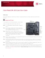
SGH-E630 Flow Chart of Troubleshooting

7-

2

DVDD 

SWITCH


AVDD


DVDD 

TYP


12C


SIM_RST


HIGH VOLTAGE


VDD_KEY


VBAT


BL_VDD


calibration


VIB 

CHARGE


GENERATO


R


VOLTAGE


LINREG


PUM

 P


VCC_SYN


supply


reference


VDD2


&


2V85


SI

 M


CHARGE


VDD_AM


P


HF 

SUPPLY & 


SIGNAL


MONITOR


INTERNAL


2V7


2V95


PLL


INTERFACE


GENERATO 

VDD1


htmp


statu

 s 

TEMP HIGH


CONTROL


2V1


MODULE


contro

 l 

CONTROL


voltage


CONTROL


1V35


(CHARGE


SUPPLY


AVDD_TEM


P


OSCILLATO


R


RF power supply


Baseband power supply


internal


RF power supply


3V05


3V25


SIGNAL


VCC_RX_BURST


3V


SIMVD


D


INTERFACE


CLOCK


BACKLIGHT


SENSOR


refgnd


PUMP

 + 

VCC_RF_VCO


32K


clocks


3V05


htmp 

internal


DVDD 

VDD_VIB


32KHz XTA


L


CLOCK


2V7


TYP


ON/OFF


data


V_ISUP


MIC BIAS


2V7


bias current


s


DVDD 

SIM_VCC


VCC_CP


2V7


SUPPLY


SIM_CLK


REAL-TIME


INTERRUPT 

AVDD 

2V65


ovdd 

4V


SI

 M


VDD3


2V35


LINREG


BATTERY


5V


MIC_BIAS


ON-CHI

 P


SIM_IO


Baseband power supply


2V85


PMU (IC)


SIM


VBAT


VDD1


VCC_CP


2V65


VCC_RX_TX


REFERENCE


2V7


NC


C505


VBAT


VCC_TX_BURST


2.2U

 F


C518


6.3V


10UF


C526


C500


VBAT


T502


100N

 F


V_ISUP


C516


100N

 F


4.7UF


C508


VCC_SYN


C528


1UF


100N

 F


C503


VBA

 T 

C522


10UF


VDD3


VBA

 T 

3.3K


U802


G


10


100NF


C501


2


3


4


5


6


7


G


G


8


9


G


VDD_VIB


AVDD_TEM


P


CN500


0-0292123-1


1


T63


NC


C519


VBA

 T 

C515


4.7UF


C517


2.2UF


R503


0


C521


T500


1UF


VDD_KEY


12PF


C512


10M


VDD2


VCC_RF_VCO


AVD

 D


R501


1U

 F


C527


C507


10NF


BLM11A102SPT


L803


C529


1UF


T501


10K


R500


F4


VSS4 

G4


VSS5 

J3


VSS6 

G5

 K5


VSS7 

VSS8 

F6

 G6


VSS9 

V_ISUP


VSS15 

VSS16 

C7

 D6


VSS17 

VSS18 

E5

 D5


VSS19 

VSS2 

F5


VSS20 

D4

 C4


VSS21 

VSS3 

A3


VPRO 

H7


VSS1 

E4


VSS10 

G7

 G8


VSS11 

VSS12 

F7

 E6


VSS13 

VSS14 

E7

 D7


B1


SIMVBAT 

B2


SLPMOD 

D1

 0


TM


H5


J5


VBACK


VBAT


K4


VCC

  C2


B3


VIBVBA 

VIBVD 

E3


SD

 A


F2


SEL12RB 

E9


SEL3RB 

H4


SIMCLK

  C6


SIMGND 

A2


B8


SIMIO


SIMSCN 

A1


SIMSC 

F9


RF2SNS


H9


RF2SW


S


E10


RF2VDD


H10


RF2VDD


S


J10


RFVBAT


G9


C1


RST


D9


RSTO 

SCL


K1


REC2 

J2


REC3 

K2


REFC


H8


REFGND


K6


RF1SNS


F10


E8


RF1SW


S


RF1VDD


G10


RF1VDD


S


H6


ISUPD


J4


MICBIAS


J6


NC


1


NC

 2


H3


ONKEY 

K8


OSC32I

  K9


OSC32O


REC1 

B9


HVSO


C


B10


HVSSCN

  A10


HVSSCP

 C9


HVSVBAT

 C8


HVSVDD

 D8


C10


IN 

IO

  D2


ISUPA


H2


DVDD4 

A4


DVDD4ON 

F8


DVDD4VBA 

B4


HFAVBA 

A5

 B5


HFAVBA 

A6


HFAVD 

HFAVD 

B6


HVSGND


D1


DVDD1 

F1


DVDD1VBA 

F3


DVDD2 

G2

 G1


DVDD2 

DVDD2VBAT 

G3


DVDD3 

H1

 J1


DVDD3 

DVDD3VBA 

C5


BLVBAT


B7


BLVD


D


A7


CHRIV

 E1


CHRREG

 E2


CHRVBAT

 D3


CLK

  C3


CLK32 

A9


CPRES


U500


K3


AUXO 

J7


AVD 

AVD 

K7


AVDDS 

K10


AVDDVBA 

J8

 J9


AVDDVBA 

BBMGN


D


A8


BBMSW


PCF50601ET1-N5


C524


100NF


C520


470N

 F


VBAT


VDD_AM


P


10U

 F


C523


100N

 F


C509


VCC_RX_TX


C506


12PF


T504


FC-255


X1


2


1


C514


1UF


4.7U

 F


C513


C502


M500


RB414_IV02N


2


NEG


1


PO

 S


470N

 F


MIC_BIAS


1U

 F


C525


VDD1


C511


100NF


1U

 F


T503


C504


C530


NC


BACKLIGH

 
T


32K


CHARGER_O

 
K


PON_SYN


JIG_REC


JACK_IN


RECO


1


ONKEY_N


IT_PM


U


VI

 B


SIMI

 O


SIMCLK


V_MOD

 E


SD

 A


SCL


RSTO


N


PON_TX


REF_O


N


Power On

Summary of Contents for SGH-E630

Page 1: ... SERVICE Manual GSM TELEPHONE CONTENTS 1 Specification 2 Circuit Description 3 Exploded Views and Parts List 4 Electrical Parts List 5 Block Diagrams 6 PCB Diagrams 7 Flow Chart of Troubleshooting GSM TELEPHONE ...

Page 2: ...onics Co Ltd Sep 2004 Printed in Korea Code No GH68 05360A BASIC ⓒ This Service Manual is a property of Samsung Electronics Co Ltd Any unauthorized use of Manual can be punished under applicable International and or domestic law ...

Page 3: ...Rx spacing 45MHz 45MHz 95MHz 80MHz Mod Bit rate Bit Period 270 833kbps 3 692us 270 833kbps 3 692us 270 833kbps 3 692us 270 833kbps 3 692us Time Slot Period Frame Period 576 9us 4 615ms 576 9us 4 615ms 576 9us 4 615ms 576 9us 4 615ms Modulation 0 3GMSK 0 3GMSK 0 3GMSK 0 3GMSK MS Power 33dBm 13dBm 33dBm 5dBm 30dBm 0dBm 30dBm 0dBm Power Class 5pcl 15pcl 5pcl 19pcl 0pcl 15pcl 0pcl 15pcl Sensitivity 10...

Page 4: ...Bm 18 7 3 dBm 19 5 3 dBm TX Power control level DCS1800 0 30 2 dBm 1 28 3 dBm 2 26 3 dBm 3 24 3 dBm 4 22 3 dBm 5 20 3 dBm 6 18 3 dBm 7 16 3 dBm 8 14 3 dBm 9 12 4 dBm 10 10 4 dBm 11 8 4dBm 12 6 4 dBm 13 4 4 dBm 14 2 5 dBm 15 0 5 dBm TX Power control level PCS1900 0 30 2 dBm 1 28 3 dBm 2 26 3 dBm 3 24 3 dBm 4 22 3 dBm 5 20 3 dBm 6 18 3 dBm 7 16 3 dBm 8 14 3 dBm 9 12 4 dBm 10 10 4 dBm 11 8 4dBm 12 6 ...

Page 5: ...emodulator and Tx IQ modulator The oscillator for RX IQ demodulator and Tx modulator are controlled by serial data to select channel and use fast lock mode for GPRS high class operation 5 UAA3536HN U100 This chip integrates two differential input LNAs The GSM input supports the E GSM DCS input supports the DCS1800 The LNA inputs are matched to the 200 ohm differential output SAW filters through et...

Page 6: ...ons work together to ensure proper system behavior during start up or in the event of a fault condition low microprocessor voltage insufficient battery energy or excessive die temperature 1 2 LCD Backlight Brightness Controler MAX1574 The Backlight Brightness is controled by Main chip OM6357_7 through the MAX1574 charge pump The MAX1574 charge pump drives three white LED s with regulated constant ...

Page 7: ...nterface pins among OM6357 KBIO 0 7 These signals compose the matrix Result of matrix informs the key status to key interface in the OM6357 Power on off key is seperated from the matrix So power on off signal is connected with PCF50601 to enable PCF50601 Key LED is consisted of four white LED for sub key and six white LED for main key Key LED use the BLVDD supply voltage Main key LED is controlled...

Page 8: ...ritten into it including incoming call melody with words that can be used for traning karaoke and commercial channel that combines texts images and sounds and others The hardware sequencer of YMU765MA5 directly interprets and plays blocks relevant to systhesis playing music and reproducing ADPCM with FM synthesizer that are included in data distributed in SMAF 5 Memory signals in the OM6357_7 enab...

Page 9: ...V317SAQ Tiger is an Integrated circuit for mobile phone camera This structure will allow effectiveness for large data management and significantly reduces main processor will get burden In hence Tiger will allow the user to be able to display to LCD direct without burdening the main processor It also allows to have various kinds of display size on the LCD and snapshot for Jpeg Digital effect will ...

Page 10: ... Parts list This Document can not be used without Samsung s authorization 3 1 1 Cellular phone Exploded View QFR01 QMW02 QFU01 QKP02 QMO01 QSP01 QMP02 QME02 QLC01 QFL01 QPC01 QKP01 QCA02 QMI01 QME01 QMP01 QCK01 QCA01 QAN02 QRE01 QIF01 QRF01 QCR31 QBA21 QCR05 QSC02 QCR26 QVK01 QVO01 QCW01 ...

Page 11: ...00098A QLC01 LCD GH07 00561A QCR26 SCREW MACHINE 6001 001850 QFR01 FRONT COVER GH75 04605A QKP01 KEYPAD MAIN GH75 04611A QIF01 IF CONN COVER GH72 15017A QMP01 MAIN PBA GH92 01889A QVK01 UNIT VOLUME KEY GH59 01436A QME01 UNIT METAL DOME GH59 01437A QCA02 UNIT CAM KEY GH59 01435A QCR05 SCREW 6001 001478 QMI01 MICROPHONE ASSY GH30 00134A QCK01 MEC CAM KEY GH75 04610A QCR31 SCREW 6001 001795 QVO01 MEC...

Page 12: ...loded view and its Part list This Document can not be used without Samsung s authorization 3 3 3 Test Jig GH80 01909A 3 1 RF Test Cable GH39 00182A 3 2 Test Cable GH39 00217A 3 3 Serial Cable 3 4 Power Supply Cable 3 5 DATA CABLE GH39 00219A 3 6 TA GH44 00483A ...

Page 13: ... 002138 U402 1205 002327 U100 1205 002350 U500 1404 001221 V600 1405 001082 V201 1405 001082 V202 1405 001082 V203 1405 001082 V204 1405 001082 V205 1405 001082 V501 1405 001082 V502 SEC CODE Design LOC 1405 001082 V601 1405 001082 V700 1405 001082 V701 1405 001082 V702 1405 001082 V703 1405 001082 V704 1405 001082 V705 1405 001082 V706 1405 001082 V707 1405 001082 V801 1405 001082 V802 1405 00108...

Page 14: ...08 2007 000162 R410 2007 000162 R411 2007 000162 R413 2007 000162 R418 2007 000162 R425 2007 000162 R428 2007 000162 R600 2007 000162 R601 2007 000162 R602 2007 000162 R603 SEC CODE Design LOC 2007 000162 R615 2007 000162 R703 2007 000162 R722 2007 000162 R728 2007 000162 R801 2007 000171 R204 2007 000171 R207 2007 000171 R424 2007 000171 R429 2007 000171 R802 2007 000171 R803 2007 000171 R804 200...

Page 15: ...10 2203 000233 C101 2203 000233 C109 2203 000233 C132 2203 000233 C137 2203 000233 C147 2203 000233 C148 2203 000233 C216 2203 000233 C217 2203 000233 C410 2203 000233 C414 SEC CODE Design LOC 2203 000233 C422 2203 000233 C825 2203 000254 C301 2203 000254 C302 2203 000254 C411 2203 000254 C413 2203 000254 C507 2203 000278 C229 2203 000278 C230 2203 000278 C701 2203 000278 C709 2203 000278 C713 220...

Page 16: ...20 2203 005050 C710 2203 005057 C123 2203 005057 C124 2203 005057 C136 2203 005061 C304 2203 005061 C305 2203 005061 C306 2203 005061 C307 2203 005061 C309 2203 005061 C310 SEC CODE Design LOC 2203 005061 C311 2203 005061 C312 2203 005061 C313 2203 005061 C314 2203 005061 C315 2203 005061 C316 2203 005061 C317 2203 005061 C318 2203 005061 C319 2203 005061 C320 2203 005061 C403 2203 005061 C404 220...

Page 17: ...02 2203 006053 C525 2203 006090 C607 2203 006093 C133 2203 006093 C138 2203 006093 C406 2203 006093 C409 2203 006093 C526 2203 006093 C530 2203 006093 C531 2203 006093 C533 SEC CODE Design LOC 2203 006093 C534 2203 006093 C706 2203 006190 C204 2203 006190 C205 2203 006190 C208 2203 006190 C405 2203 006208 C502 2203 006208 C508 2203 006208 C510 2203 006208 C515 2203 006208 C517 2203 006208 C518 220...

Page 18: ...01362 L301 3301 001362 L400 3301 001438 L700 3301 001438 L701 3301 001438 R741 3301 001438 R742 3705 001287 CN201 3711 005558 CN603 4302 001130 M500 GH13 00020A U400 S U B SEC CODE Design LOC 0403 001427 ZD1 0407 001002 D1 0601 001819 D2 0601 001819 D3 0601 001819 D4 0601 001819 D5 1405 001082 V1 1405 001082 V2 1405 001082 V3 1405 001082 V4 1405 001082 V5 1405 001082 V6 1405 001082 V7 1405 001082 ...

Page 19: ...SAMSUNG Proprietary Contents may change without notice This Document can not be used without Samsung s authorization 5 SGH E630 Block Diagrams 5 1 1 RF Solution Block Diagram ...

Page 20: ...AMP Charging Circuit Li Ion Battery Standard OM6357_7 VIBRATOR SYSTEM CLOCK 13MHz RTC_CLOCK 32 768KHz KEY_BOARD RECEIVER MIC LCD RF INTERFACE VCC_RX_TX VCC_RF_VCO VCC_TX_BURST PMU VCC_SYN Serial Data Interface I O Interface A D Interface BB INTERFACE MELODY IC 64 Poly SPEAKER VDD1 VDD2 VDD3 VDD_VIB MIC_BIAS VCC_CP VDD_KEY VDD_AMP AVDD AVDD_TEMP SIM CARD BL_VDD FLASH NOR 128M bit NAND 256M 256M bit...

Page 21: ...SAMSUNG Proprietary Contents may change without notice This Document can not be used without Samsung s authorization 6 SGH E630 PCB Diagrams 6 1 1 Main PCB Top Diagram ...

Page 22: ...SAMSUNG Proprietary Contents may change without notice PCB Diagrams This Document can not be used without Samsung s authorization 6 2 2 Main PCB Bottom Diagram ...

Page 23: ... more than 3 4V Power On does not work Change the Battery END No Yes C513 V_ISUP 2 7V Check the PMU related to V_ISUP No Yes Check the Clock at R501 32KHZ Resolder X1 No Yes C530 VDD1 H Check the VDD1 circuit No Yes C529 VDD2 C528 VDD3 2 8V Check the VDD2 VDD3 circuit No Yes Check for the clock at C137 13MHz Check the clock generation circuit related to U100 No Yes Check the initial operation Yes ...

Page 24: ...UF C517 2 2UF R503 0 C521 T500 1UF VDD_KEY 12PF C512 10M VDD2 VCC_RF_VCO AVD D R501 1U F C527 C507 10NF BLM11A102SPT L803 C529 1UF T501 10K R500 F4 VSS4 G4 VSS5 J3 VSS6 G5 K5 VSS7 VSS8 F6 G6 VSS9 V_ISUP VSS15 VSS16 C7 D6 VSS17 VSS18 E5 D5 VSS19 VSS2 F5 VSS20 D4 C4 VSS21 VSS3 A3 VPRO G H7 VSS1 E4 VSS10 G7 G8 VSS11 VSS12 F7 E6 VSS13 VSS14 E7 D7 B1 SIMVBAT B2 SLPMOD D1 0 TM H5 J5 VBACK VBAT K4 VCC C2...

Page 25: ...Troubleshooting This Document can not be used without Samsung s authorization 7 3 2 Initial R300 RSTON H Initial Failure Check the circuit related to reset END No Yes Is U403 pin 4 6 memory CE OK Yes Yes No Check the U403 Check the circuit around LCD U403 Short or not solder Yes ...

Page 26: ...HA3 L4 N3 HA4 HA5 K5 M3 HA6 HA7 P2 N2 HA14 HA15 J5 K3 HA16 HA17 J4 K4 HA18 HA19 K2 P3 HA2 G4 HA20 P5 N8 L10 GPON 1 N9 GPON 2 HA1 M4 N1 HA10 HA11 L2 L1 HA12 HA13 M2 J2 GPIO10 L8 GPIO 2 M9 GPIO 3 P7 GPIO 4 GPIO 5 L7 L9 GPIO 6 GPIO 7 N7 P6 GPIO 8 GPIO 9 CS_N 1 CS_N 2 M5 G3 CS_N 3 CTS0_N B5 EARN A11 B10 EARP GPIO 0 M1 2 K9 GPIO 1 K8 D8 CD I CD O E9 CEN D9 P11 CKI CKI32I P13 P14 CKI32O CS_N 0 N4 G5 AUX...

Page 27: ...be used without Samsung s authorization 7 5 3 Charging Part Check the C605 4 9V Abnormal charging part END No Yes U602 pin 8 H No Yes Check the C601 4 2V No Yes Check the the circuit related to DC_VOLT Resolder or replace U602 Check the circuit related to CHG_ON signal Yes U602 pin 5 L Yes No Resolder or replace U602 ...

Page 28: ...on SGH E630 Flow Chart of Troubleshooting 7 6 Charging MES_BATT DCVOLT CHG_O N END_OF_CHARGE CHARGER_OK VBAT 330K 6 3V 10U F 10V C605 R606 220K 7 BATT G 9 MAX1508ETA U602 C601 10U F R605 VDD2 47K R604 C606 470nF R610 2 4K 1 NC R609 VDD2 C604 100PF 8 _EN 5 C602 NC 10 GG 11 12 G GND 3 IN 2 ISET 4 1 VL _ACO K 6 _CH G ...

Page 29: ... be used without Samsung s authorization 7 7 4 SIM Part CN500 pin 1 5 H Phone can t access SIM Card Check the sim charge pump Check the SIM Card END No Yes Yes Yes No Check the 32k OSC After Power ON Check SIMCLK Signal on CN500 pin3 in a few second Yes No Replace PBA After SIM card insert CN500 pin 2 H SIM_RST Yes ...

Page 30: ...Samsung s authorization SGH E630 Flow Chart of Troubleshooting 7 8 5 Microphone Part Check the connection from MIC Check the circuit from U1102 to MIC Resolder MIC Resolder the L700 L701 R704 R708 C707 and C712 END No Yes Yes Yes Yes No Check the MIC No Replace the MIC Microphone does not work ...

Page 31: ...without Samsung s authorization 7 9 Microphone MIC_BIAS R708 1 2 MI C M700 R704 1 2K NC 2 2K 47PF C700 C710 1 8PF 10PF C701 10PF C713 C714 10K 1K V705 VC040205X150R C709 10PF 10PF MIC_N MIC_P C707 R706 NC C711 BLM10B750SBPT L700 VC040205X150R V700 10PF C708 L701 BLM10B750SBPT 4V 33UF NC C703 R700 C715 C702 100N F 100N F C712 ...

Page 32: ...Melody U409 pin 5 2 85V Speaker does not work Check the Clock signal at Pin 1 of U402 26MHz Check the clock generation circuit related to U101 and U402 END No Yes No Resolder or replace U409 U402 pin 17 18 1 8V When U402 operate Resolder U402 Yes No CN606 pin 23 25 1 8V Check the circuit related to SPK_P SPK_N signal Yes No Is Speaker working No Yes Change the Speaker Yes Yes ...

Page 33: ...N F M_LED VDD2 3 3K MEL_13M M_RST HA 1 MELODY_C S AMP_N R401 330 R403 10V C408 C402 1N F VDD2 100N F C404 C420 100N F VDD3 100PF C400 C405 220N F 27PF C401 U402 YMU762 MA 3 R406 6 8K 220N F C419 R405 1 2K U409 TC7SH04FU TE85L 3 18 SPOUT 2 SPVD D 15 16 SPVSS VDD 7 VREF 9 VS S 8 29 C S IRQ 3 14 EQ 3 10 HPOUT L MON O HPOUT R 11 32 IOVDD 2 LED MT R 19 NC 5 6 PLLC SPOUT 1 17 24 D3 D4 23 22 D5 D6 21 20 ...

Page 34: ...without Samsung s authorization SGH E630 Flow Chart of Troubleshooting 7 12 7 Key Data Input When one of the keys is pushed is it displayed on LCD Check the Dome sheet Key Pad END No Yes Yes Check Initial Operation When one of the keys is pushed KBIO signal is OK Replace the PBA No Yes ...

Page 35: ...02 pin 1 5 1 5V Resolder R727 R730 U702 END No Yes Yes Receiver does not work CN606 pin 23 25 1 5V Replace the CN606 No Yes Is Receiver working Replace the Receiver No Yes No Resolder U702 Yes No Resolder or replace U702 U702 pin 4 16 1 5V Yes CN604 pin 8 9 short No Resolder CN604 Yes Check the soldering of the speaker FPC No Modufy the speaker FPC soldering Yes U702 pin 2 10 H ...

Page 36: ...g s authorization SGH E630 Flow Chart of Troubleshooting 7 14 9 LCD Part Is LCD Contrast set on high level in the Menu Set LCD Contrast on high level END No Yes Yes LCD does not work CN606 pin 21 2 8V Check the R315 No Yes CN606 pin 19 L_WR 20 RS is OK Check the U400 No Yes Yes Replace the LCD Module ...

Page 37: ...ing This Document can not be used without Samsung s authorization 7 15 10 Key Back Light 1 Main Key Part C524 H Check the PMU related to VDD_KEY END No Yes Yes Main Key Backlight does not work 2 Sub Key Part C531 H Check the PMU related to BLVDD END No Yes Sub Key Backlight does not work Yes ...

Page 38: ...shooting 7 16 11 Camera part Camera function does not work Yes No Connect the camera module Check the Camera connector on Main Board Yes CN606 pin 29 31 2 8V No Check LCD and CN606 Yes U101 Pin 3 U409 Pin 4 26MHz No Check U101 U409 and C410 C422 Yes CN606 pin 21 2 8V Yes No Check the R315 Is there another problem END Replace the camera module Yes ...

Page 39: ...Pin8 65dBm Resolder CN201 R1120 C202 END No Yes RX ON RF input center freq 947 4 MHz Amp 50dBm Check U205 pin10 L pin12 L pin9 L U205 pin5 pin6 65dBm U100 pin 6 7 8 9 1V U100 pin32 70dBm pin33 70dBm Check ANT Switch control circuit Resoder U205 Resolder L100 L101 L102 Resolder U100 or Check pins related to U100 R116 R117 R118 R119 1V Yes Yes Yes Yes Yes Yes No No No No Check U1102 ...

Page 40: ...5Level Check U205 pin11 H 2 68V pin12 L pin9 L U205 pin8 20dBm U201 pin12 20dBm osc401 pin1 8dBm U201 pin6 11dBm Change or Resolder U205 Check ANT Switch control circuit Resolder C203 Resolder R204 U100 pin6 7 8 9 500mV Yes Check U201 VBATT C212 R204 OK Resolder or Change U201 Check VBATT or PAM control signal No No No No No No No Yes Yes Yes Yes Yes Yes Yes Yes END Check U1102 Resolder U100 or Ch...

Page 41: ...in8 65dBm Resolder CN201 C202 R1120 No Yes RX ON RF input CH center freq 1842 4 MHz Amp 50dBm Check U205 pin10 L pin12 L pin9 L U205 pin1 pin2 65dBm U100 pin6 7 8 9 1V U100 pin38 70dBm pin39 70dBm Check ANT Switch control circuit Resoder U205 Resolder L104 L105 L107 R116 R117 R118 R119 1V Yes Yes Yes Yes Yes Yes No No No No END Check U1102 Resolder U100 or Check pins related to U100 ...

Page 42: ...vel Check U205 pin10 L pin9 L pin12 H 2 68V U205 pin8 13dBm U201 pin17 13dBm osc401 pin5 12dBm U201 pin5 15dBm Change or Resolder U205 Check ANT Switch control circuit Resolder C1127 Resolder R207 U100 pin 6 7 8 9 500mV Yes Check U201 VBATT C212 R204 OK Resolder or Change U201 Check VBATT or PAM control signal No No No No No No No No Yes Yes Yes Yes Yes Yes Yes Yes END Check U1102 Resolder U100 or...

Page 43: ...1 16 PCS Receiver U205 Pin8 65dBm Resolder CN201 C202 R1120 No Yes RX ON RF input CH center freq 1960 MHz Amp 50dBm Check U205 pin10 L pin12 L pin9 H U205 pin3 pin4 65dBm U100 pin6 7 8 9 1V Resolder C151 C152 L108 R116 R117 R118 R119 1V Yes Yes Yes Yes Yes Yes No No No No END Check U1102 Resolder U100 or Check pins related to U100 U100 pin38 70dBm pin39 70dBm ...

Page 44: ...vel Check U205 pin10 L pin9 L pin12 H 2 68V U205 pin8 13dBm U201 pin17 13dBm osc401 pin5 12dBm U201 pin5 15dBm Change or Resolder U205 Check ANT Switch control circuit Resolder C1127 Resolder R207 U100 pin 6 7 8 9 500mV Yes Check U201 VBATT C212 R204 OK Resolder or Change U201 Check VBATT or PAM control signal No No No No No No No No Yes Yes Yes Yes Yes Yes Yes Yes END Check U1102 Resolder U100 or...

Reviews: