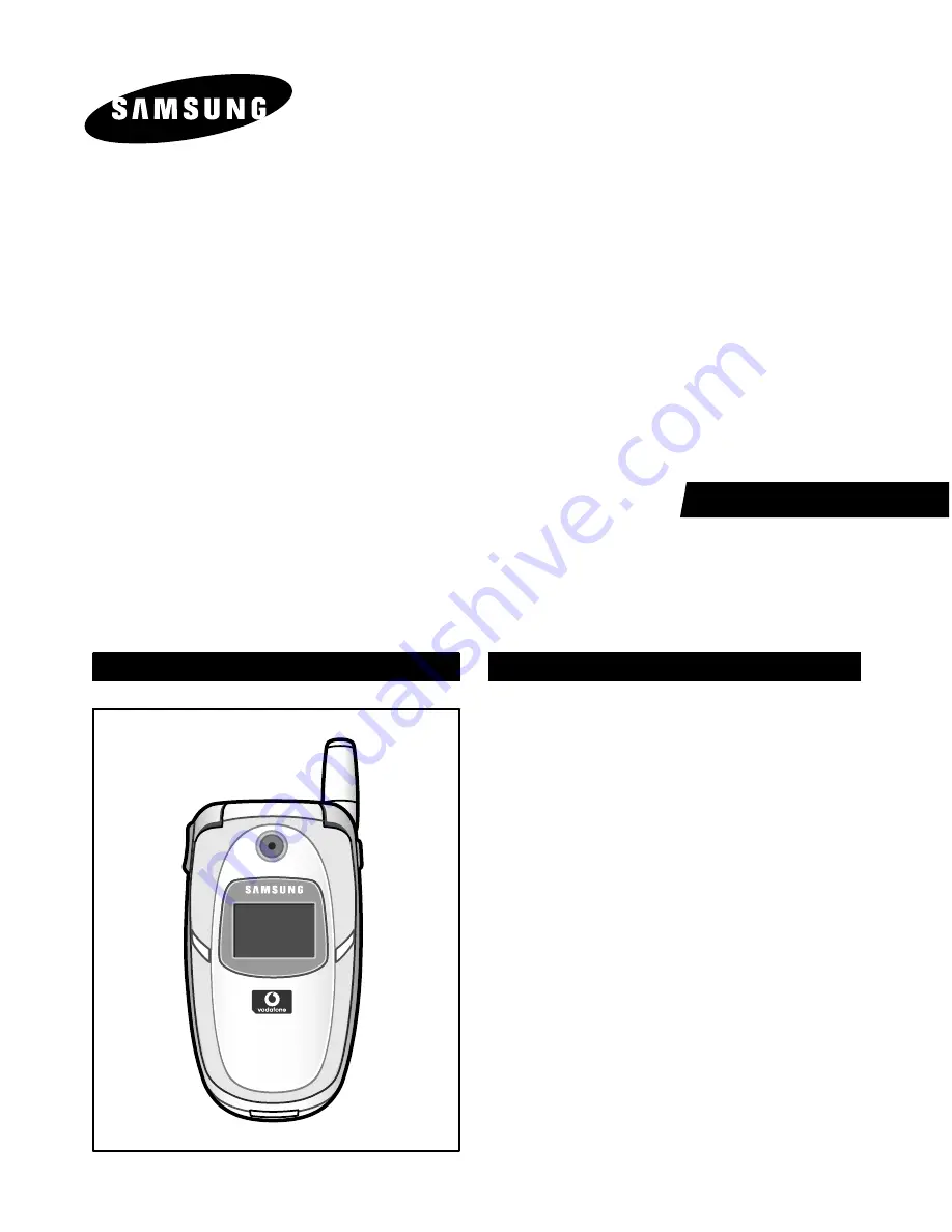
GSM TELEPHONE
SGH-E310
CONTENTS
1.
Specification
2.
Flow Chart of Troubleshooting
3.
Exploded Views and Parts List
4.
Electrical Parts List
5.
Block Diagrams
6.
PCB Diagrams
SERVICE
Manual
Page 1: ...GSM TELEPHONE SGH E310 GSM TELEPHONE CONTENTS 1 Specification 2 Flow Chart of Troubleshooting 3 Exploded Views and Parts List 4 Electrical Parts List 5 Block Diagrams 6 PCB Diagrams SERVICE Manual ...
Page 2: ...24 975 1023 512 885 512 810 Tx Rx spacing 45MHz 45MHz 95MHz 80MHz Mod Bit rate Bit Period 270 833kbps 3 692us 270 833kbps 3 692us 270 833kbps 3 692us 270 833kbps 3 692us Time Slot Period Frame Period 576 9us 4 615ms 576 9us 4 615ms 576 9us 4 615ms 576 9us 4 615ms Modulation 0 3GMSK 0 3GMSK 0 3GMSK 0 3GMSK MS Power 33dBm 13dBm 33dBm 5dBm 30dBm 0dBm 30dBm 0dBm Power Class 5pcl 15pcl 5pcl 19pcl 0pcl ...
Page 3: ...15 13 2 dBm 16 11 3 dBm 17 9 3dBm 18 7 3 dBm 19 5 3 dBm TX Power control level DCS1800 0 30 3 dBm 1 28 3 dBm 2 26 3 dBm 3 24 3 dBm 4 22 3 dBm 5 20 3 dBm 6 18 3 dBm 7 16 3 dBm 8 14 3 dBm 9 12 4 dBm 10 10 4 dBm 11 8 4dBm 12 6 4 dBm 13 4 4 dBm 14 2 5 dBm 15 0 5 dBm TX Power control level PCS1900 0 30 3 dBm 1 28 3 dBm 2 26 3 dBm 3 24 3 dBm 4 22 3 dBm 5 20 3 dBm 6 18 3 dBm 7 16 3 dBm 8 14 3 dBm 9 12 4 ...
Page 4: ...re than 100mA Power On does not work Check the Voltage more than 3 3V Download again Charge the Battery Check the pin 11 of U102 is more than 2 8V Check U102 and C117 U102 pin 39 2 8V Check U102 and C116 Check the clock signal at pin4 of OSC801 Freq 13MHz Vrms 300mV Vpp is around 900mVpp Check the clock generation circuit Check the initial operation END No Yes Yes Yes Yes Yes Yes No No No No U102 ...
Page 5: ... U701 Check the pin 4 of OSC801 is around 2 8V Check the soldered status of OSC801 R801 U102 Yes No Yes Check LCD connector CN201 and resolder bridge Yes No Check the pin 1 of CN101 voltage 3V Phone can t access SIM card Check the SIM connector s CN101 connection to SIM card Check the circuit related to U102 Resolder or change CN101 Check the circuit around CN101 input circuitry END No Yes Yes Yes...
Page 6: ...4 Charging Part Check the pin 17 18 of CN300 is TA_VEXT 4 Abnormal charging part Check the pin 2 of Q102 is low Replace TA Check CN300 Check the Q102 Check the Q100 END No Yes Yes Yes Yes No No Check the pin 3 of Q100 is low Check the pin 5 of Q102 is 3 2 4 2V Check the Q102 No Yes Check the ICHRG is 1V during charging and around 180mV full charging No Resolder or change R102 Yes ...
Page 7: ...SAMSUNG Proprietary Contents may change without notice SGH E310 Flow Chart of Troubleshooting and Circuit Diagrams 2 4 This Document can not be used without Samsung s authorization Picture 1 ...
Page 8: ...SAMSUNG Proprietary Contents may change without notice SGH E310 Flow Chart of Troubleshooting and Circuit Diagrams 2 5 This Document can not be used without Samsung s authorization Picture 2 ...
Page 9: ...SAMSUNG Proprietary Contents may change without notice SGH E310 Flow Chart of Troubleshooting and Circuit Diagrams 2 6 This Document can not be used without Samsung s authorization Picture 3 ...
Page 10: ...phone Microphone does not work Check the reference voltage on mic path C431 2 0 V Resolder microphone Resolder or change R424 C431 R413 C410 R408 R411 END No Yes Yes Yes Yes No Is microphone ok No Check U701 Check the connection from CN201 to LCD module Speaker does not work Check the PIN 4 and PIN 8 of U401 High Check the circuit related to U401 Check U601 Is speaker ok Check U701 END No Yes Yes ...
Page 11: ...SAMSUNG Proprietary Contents may change without notice SGH E310 Flow Chart of Troubleshooting and Circuit Diagrams 2 8 This Document can not be used without Samsung s authorization ...
Page 12: ...ng and Circuit Diagrams 2 9 This Document can not be used without Samsung s authorization 7 Camera Part Camera function dose not work Yes Check the connect CN201 Yes U1002 PIN 9 10 2 8V Yes R1020 25MHz Connect the camera module Check U1002 and C1022 C1021 Check U1001 and OSC1000 No No No END ...
Page 13: ...SAMSUNG Proprietary Contents may change without notice SGH E310 Flow Chart of Troubleshooting and Circuit Diagrams 2 10 This Document can not be used without Samsung s authorization ...
Page 14: ...PUT 62CH AMP 50dBm NORMAL CONDITION catch the channel CHECK ANT701 L905 contact U800 pin 9 32 2 8V F900 CHECK pin2 3 65dBm U800 CHECK pin20 21 65dBm C900 F901 resolder or change F900 resolder or change C912 C913 L901 resolder or change U102 pin39 C112 change or resolder U800 CHECK pin 8 13MHz Vp p 950mV OSC801 change or resolder U800 resolder or change U701 CHECK U800 pin1 2 3 28 Vp p 120mV NO YES...
Page 15: ... 698CH AMP 50dBm NORMAL CONDITION catch the channel CHECK ANT701 L905 contact U800 pin 9 32 2 8V F900 CHECK pin4 5 65dBm U800 CHECK pin18 19 65dBm C900 F901 resolder or change F900 resolder or change C914 C915 L902 resolder or change U102 pin39 C112 change or resolder U800 CHECK pin 8 13MHz Vp p 950mV OSC801 change or resolder U800 resolder or change U701 CHECK U800 pin1 2 3 28 Vp p 120mV NO YES N...
Page 16: ...heck change U900 pin8 20 3 7 V NO NO YES YES YES NO NO BATTERY U102 check change U900 pin 22 1 6V YES NO U900 pin6 about 5dBm YES U900 pin 2 3V YES YES U900 change or resolder NO U701 check U701 check NO U800 pin9 32 2 8V U102 pin39 C112 change or resolder YES U800 pin8 13MHz Vp p 950mV U800 pin4 5 6 7 100mV YES U701 change or resolder NO NO U800 change or resolder YES NO OSC801 change or resolder...
Page 17: ...change U900 pin8 20 3 7 V NO NO YES YES YES NO NO BATTERY U102 check change U900 pin 22 1 4V YES NO U900 pin5 about 5dBm YES U900 pin 2 3V YES YES U900 change or resolder NO U701 check U701 check NO U800 pin9 32 2 8V U102 pin39 C112 change or resolder YES U800 pin8 13MHz Vp p 950mV U800 pin4 5 6 7 100mV YES U701 change or resolder NO NO U800 change or resolder YES NO OSC801 change or resolder CONT...
Page 18: ...SAMSUNG Proprietary Contents may change without notice SGH E310 Flow Chart of Troubleshooting and Circuit Diagrams 2 15 This Document can not be used without Samsung s authorization Picture 1 ...
Page 19: ...SAMSUNG Proprietary Contents may change without notice SGH E310 Flow Chart of Troubleshooting and Circuit Diagrams 2 16 This Document can not be used without Samsung s authorization Picture 2 ...
Page 20: ...SAMSUNG Proprietary Contents may change without notice SGH E310 Flow Chart of Troubleshooting and Circuit Diagrams 2 17 This Document can not be used without Samsung s authorization Picture 3 ...
Page 21: ...w and its Parts list 3 1 This Document can not be used without Samsung s authorization 1 Cellular phone Exploded View QFR01 QWD01 QFU01 QLC371 QSP01 QMO02 QCA01 QFL01 QMW01 QCR04 QSC05 QSC08 QVO01 QMP01 QVK01 QCA02 QME02 QMI01 QIF02 QKP01 QMP01 QRE01 QCK01 QCR06 QSC03 QMP01 QBA21 ...
Page 22: ... QMW01 LCD WINDOW ASSY GH75 03874A QCR04 SCREW 6001 001479 QSC05 SCREW SHEET L GH74 06886A QSC08 SCREW SHEET R GH74 06867A QFR01 FRONT COVER GH75 03867A QVO01 VOLUME KEY GH75 04736A QKP01 KEYPAD GH75 03939A QMP01 PBA MAIN GH92 01746A QVK01 UNIT VOLKEY GH59 01016A QCA02 CAMERA KEY GH59 01458A QME02 METAL DOME GH59 01097A QMI01 MICROPHONE GH30 00062A QIF02 IF COVER GH73 01394F QCK01 CAMERA KEY GH75 ...
Page 23: ... Exploded view and its Part list 3 3 This Document can not be used without Samsung s authorization 3 Test Jig GH80 00865A 3 1 RF Test Cable GH39 00090A 3 2 Test Cable GH39 00127A 3 3 Serial Cable 3 4 Power Supply Cable 3 5 DATA CABLE GH39 00159A 3 6 TA GH44 00184A ...
Page 24: ...0812 C214 2203 000812 C215 2203 000812 C216 2203 005682 C217 2203 005682 C218 2203 000812 C219 2203 005682 C220 2203 000812 C221 2203 005682 C222 2203 005682 C223 2203 005682 C225 2203 005682 C226 2203 005682 C227 2203 005682 C230 2203 000812 C231 2203 005682 C232 2203 000812 C233 2203 005682 C234 2203 005682 C235 2203 005682 C236 2203 005682 C237 2203 005682 C238 2203 005682 C239 2203 005682 C240...
Page 25: ...8 C902 2203 000995 C903 2203 002677 C904 2203 000254 C905 2203 000812 C906 2203 000254 C907 2404 001151 C909 2404 001151 C910 2203 005234 C912 2203 005234 C913 2203 005234 C914 2203 005234 C915 2203 000233 C916 2203 001383 C918 2203 000812 C919 3709 001229 CN101 3711 005490 CN201 3710 001673 CN300 3722 002082 CN400 2909 001225 F900 3705 001287 F901 2703 001513 L402 2703 001513 L403 2703 002485 L90...
Page 26: ...2007 000148 R423 2007 000140 R424 2007 000172 R425 2007 000171 R500 2007 000157 R501 2007 000171 R502 2007 000172 R503 2007 000157 R601 2007 000172 R602 2007 000170 R603 2007 000157 R604 2007 000157 R605 2007 007142 R606 2007 007308 R607 2007 007308 R608 2007 000162 R701 2007 007200 R702 2007 007200 R703 2007 000162 R704 2007 000172 R801 2007 007766 R802 2007 001313 R803 2007 000138 R804 2007 0012...
Page 27: ...ice SGH E310 Electrical Parts List 4 4 This Document can not be used without Samsung s authorization SEC Code Design LOC GH30 00062A GH59 01016A GH59 01097A GH59 01458A GH68 02026A GH73 03030A GH73 03033A GH74 07565A GH74 07566A GH74 07567A GH74 08170A ...
Page 28: ...Solution Block Diagram Antenna ASM RF FILTER π 2 RF PLL PGA SERIAL DATA INTERFACE GSM 890MHz 915MHz PAM GSM 925MHz 960MHz I Q CSP1093 TRIDENT DSP16000 ARM7TDMI UI SERIAL DATA CLK LE RF FILTER DCS 1805MHz 1880MHz L N A PGA A D C A D C IF PLL DCS 1710MHz 1785MHz D E T 100KHz CHANNEL FILTER D A C D A C PGA PGA R X TCVCXO 13 MHz C L K A F C T X I Q Si 4205 ...
Page 29: ... VCO IF VCO GPIO POWER DC DC CHARGER SIM X TAL 13MHz RS232 CSP1093 Audio Part LCD KEYBOARD SRAM 32M FLASH ROM 128M TXIP TXIN TXQP TXQN RXIP RXIN RXQP RXQN SERCK SERLE SERDA RFOVL TXP OCTL RF DIRVER TXI Q RX I Q TXP SERCK SERLE SERDA OCTL IO RWN AB 8 0 DB 15 0 INT1 IRQx PAx RSTB IO RWN AB 8 0 DB 15 0 INT1 IRQx PAx RSTB ARM JTAG ICE DAICK DAIRN DAIDO DAIDI DAI DSPJTAG JTAG GPRS ACC PPI Programmable ...
Page 30: ...C611 C612 C613 C614 C615 C701 C704 C705 C706 C707 C708 C709 C710 C711 C712 C801 C802 C803 C804 C805 C806 C807 C808 C809 C810 C811 C812 C813 C814 C900 C901 C902 C903 C904 C905 C906 C907 C909 C910 C911 C912 C913 C914 C915 C916 C917 C918 C919 CN101 CN201 CN300 CN400 F900 F901 G1 G2 G3 G4 L402 L403 L900 L901 L902 L905 L906 L907 L908 LED217 M101 OSC1000 OSC601 OSC801 PWM Q100 Q103 Q401 R1001 R1002 R100...
Page 31: ... C219 C221 C231 C233 C242 C253 C255 C404 C411 C415 CLEAR CN203 CP_TCK CP_TDI CP_TDO CP_TMS DOWN END_PWD F1 F2 F3 F4 F_WE_1 G ND_2 I LED201 LED202 LED203 LED204 LED205 LED207 LED208 LED210 LED211 LED212 LED213 LED214 LED218 LED219 LED220 LED221 LED222 LEFT MIC401 Q102 Q104 R103 R112 R315 R316 R317 R401 R403 RIGHT SEND SIDE TCK_1 TDI_1 TDO_1 TMS_1 TP602 TRST_1 U1008 U1009 U202 U401 UP ZD206 ZD207 ZD...
Page 32: ...nics Co Ltd JUNE 2004 Printed in Korea Code No GH68 05560A BASIC ⓒ This Service Manual is a property of Samsung Electronics Co Ltd Any unauthorized use of Manual can be punished under applicable International and or domestic law ...