
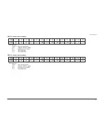


10 Operating Instructions and Installation
10-1
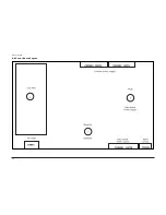
10 Operating Instructions and Installation
10-1 Front
1. SOURCE
Toggles between all the available input sources
(TV, Ext.1 , Ext.2, AV, S-Video, Component, PC,
HDMI1, HDMI2).
In the on-screen menu, use this button as you use the
ENTER button on the remote control.
2. MENU
Press to see an on-screen menu of your TV's features.
3.
Press to decrease or increase the volume.
In the on-screen menu, use the
buttons as
you use the and buttons on the remote control.
4. C/P.
Press to change channels.
In the on-screen menu, use the C/P. buttons
as you use the and buttons on the remote control.
(Without the Remote Control, you can turn on the TV
by using the Channel buttons.)
5. Speakers
6. (POWER)
Press to turn the TV on and off.
Power Indicator
Blinks and turns off when the power is on and lights
up in stand-by mode.
7. Rremote Control Sensor
Aim the remote control towards this spot on the TV.
- The product colour and shape may vary depending on the model.
Summary of Contents for LE40M91B
Page 3: ...Contents ...
Page 4: ...Contents ...
Page 27: ...4 Troubleshooting 4 4 WAVEFORMS 1 R G B Output Signal of IC500 ...
Page 29: ...4 Troubleshooting 4 6 2 Digital Output Data of IC500 3 Signal of HDMI Data ...
Page 31: ...4 Troubleshooting 4 8 WAVEFORMS 4 Tuner_CVBS Output Signal 3 CVBS Output Signal ...
Page 33: ...4 Troubleshooting 4 10 WAVEFORMS 4 CVBS Output Signal ...
Page 35: ...4 Troubleshooting 4 12 2 Digital Output Data of IC500 5 Analog Signal Y C to IC500 WAVEFORMS ...
Page 37: ...4 Troubleshooting 4 14 WAVEFORMS 6 The Signal are Inputed to IC1015 7 DC 12V ...
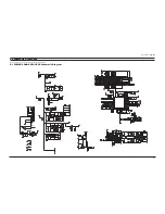
Page 69: ...8 1 8 Wiring Diagrams 8 Wiring Diagram 8 1 LE40M91BX Wiring Diagram ...
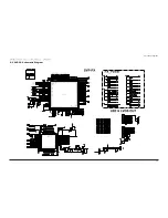
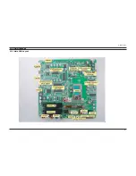
Page 70: ...8 Wiring Diagrams 8 2 8 2 Main Board Layout ...
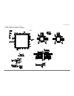
Page 74: ...8 Wiring Diagrams 8 6 8 4 Power Board Layout ...
Page 77: ...8 9 8 Wiring Diagrams ...
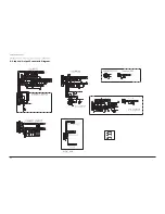
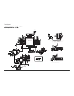
Page 81: ...9 Schematic Diagrams 9 2 9 2 Input Output Schematic Diagram ...
Page 82: ...9 Schematic Diagrams 9 3 9 3 Input Output Schematic Diagram ...
Page 83: ...9 Schematic Diagrams 9 4 9 4 Micom Schematic Diagram ...
Page 84: ...9 Schematic Diagrams 9 5 9 5 SVP PX Schematic Diagram ...
Page 85: ...9 Schematic Diagrams 9 6 9 6 Application Schematic Diagram ...
Page 86: ...9 Schematic Diagrams 9 7 9 7 FRCH 100Hz LVDS Schematic Diagram ...
Page 87: ...9 Schematic Diagrams 9 8 Memo ...
Page 98: ...12 PCB Diagram 12 1 12 PCB Diagram 12 1 Main PCB Layout ...