8 Wiring Diagrams
8-4
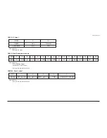
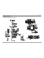
CN221 - Front control
PIN
1
2
3
4
5
6
7
8
9
10
11
12
13
14
15
NAME SDA-T SCL-T GND
KEY
LED
GND
A5V
GND
IR
KEY
KEY
GND IDENT HP-L HP-R
INPUT1
INPUT1 INPUT2
HP
Function Define
- A5V
Front control board poewr supply
- KEY INPUT1,2
Key control, from the memu, change up/down Etc.
- IR
Remote control signal
- LED
Control the timing and stand by LED color
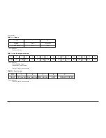
CN501 - Panel control
PIN
1
2
3
4
5
NAME
SW_inverter
Ana_dimming PWM_dimming
GND
Sensor_Power
Function Define
- SW_inverter
panel inverter control, about 3.3V
- Ana_dimming
panel dimming control
- PWM_dimming
panel PWM control, duty 40% ~ 90%
Summary of Contents for LE40M91B
Page 3: ...Contents ...
Page 4: ...Contents ...
Page 27: ...4 Troubleshooting 4 4 WAVEFORMS 1 R G B Output Signal of IC500 ...
Page 29: ...4 Troubleshooting 4 6 2 Digital Output Data of IC500 3 Signal of HDMI Data ...
Page 31: ...4 Troubleshooting 4 8 WAVEFORMS 4 Tuner_CVBS Output Signal 3 CVBS Output Signal ...
Page 33: ...4 Troubleshooting 4 10 WAVEFORMS 4 CVBS Output Signal ...
Page 35: ...4 Troubleshooting 4 12 2 Digital Output Data of IC500 5 Analog Signal Y C to IC500 WAVEFORMS ...
Page 37: ...4 Troubleshooting 4 14 WAVEFORMS 6 The Signal are Inputed to IC1015 7 DC 12V ...
Page 69: ...8 1 8 Wiring Diagrams 8 Wiring Diagram 8 1 LE40M91BX Wiring Diagram ...
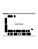
Page 70: ...8 Wiring Diagrams 8 2 8 2 Main Board Layout ...
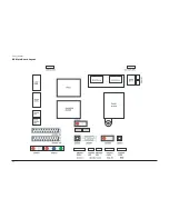
Page 74: ...8 Wiring Diagrams 8 6 8 4 Power Board Layout ...
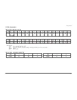
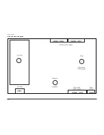
Page 77: ...8 9 8 Wiring Diagrams ...
Page 81: ...9 Schematic Diagrams 9 2 9 2 Input Output Schematic Diagram ...
Page 82: ...9 Schematic Diagrams 9 3 9 3 Input Output Schematic Diagram ...
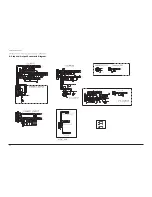
Page 83: ...9 Schematic Diagrams 9 4 9 4 Micom Schematic Diagram ...
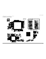
Page 84: ...9 Schematic Diagrams 9 5 9 5 SVP PX Schematic Diagram ...
Page 85: ...9 Schematic Diagrams 9 6 9 6 Application Schematic Diagram ...
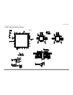
Page 86: ...9 Schematic Diagrams 9 7 9 7 FRCH 100Hz LVDS Schematic Diagram ...
Page 87: ...9 Schematic Diagrams 9 8 Memo ...
Page 98: ...12 PCB Diagram 12 1 12 PCB Diagram 12 1 Main PCB Layout ...

