4 Troubleshooting
4-3
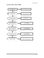
4-2-2 No Video (Analog PC)
Check a PC source and check
the connection of DSUB cable?
Input a analog PC signal and
connected cable(DPMS).
Yes
Does the signal appear at
#30, 22, 38(R, G, B) of
IC4001?
PC cable. Change a PC
cable. Change a main PCB ass'y.
Yes
Power Indicator is off.
Lamp on, no video.
No
No
1
Does the digital data appear
at the input of
LBE (RA6053~5)?
Check IC4001
Change a main PCB ass'y.
Yes
Yes
No
Yes
Check a LVDS cable?
Replace a lcd panel?
Please, Call to Samsung Co. LTD.
No
Does the digital data appear
at the output of IC4003
(RA6019_FRC~6021_FRC)?
Check IC4003
Change a main PCB ass'y.
No
Does the digital data appear
at the input of IC6003, 6004
(RA6001_FRC~RA6003_FRC,
RA6005_FRC, RA6009_FRC,
RA6016_FRC, RA6018_FRC)?
Check IC6005
Change a main PCB ass'y.
Yes
Does the digital data appear
at the out of L6001~12?
Check IC6003,4
Change a main PCB ass'y.
Yes
No
No
Summary of Contents for LE40M91B
Page 3: ...Contents ...
Page 4: ...Contents ...
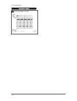
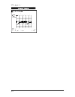
Page 27: ...4 Troubleshooting 4 4 WAVEFORMS 1 R G B Output Signal of IC500 ...
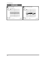
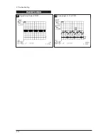
Page 29: ...4 Troubleshooting 4 6 2 Digital Output Data of IC500 3 Signal of HDMI Data ...
Page 31: ...4 Troubleshooting 4 8 WAVEFORMS 4 Tuner_CVBS Output Signal 3 CVBS Output Signal ...
Page 33: ...4 Troubleshooting 4 10 WAVEFORMS 4 CVBS Output Signal ...
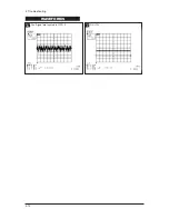
Page 35: ...4 Troubleshooting 4 12 2 Digital Output Data of IC500 5 Analog Signal Y C to IC500 WAVEFORMS ...
Page 37: ...4 Troubleshooting 4 14 WAVEFORMS 6 The Signal are Inputed to IC1015 7 DC 12V ...
Page 69: ...8 1 8 Wiring Diagrams 8 Wiring Diagram 8 1 LE40M91BX Wiring Diagram ...
Page 70: ...8 Wiring Diagrams 8 2 8 2 Main Board Layout ...
Page 74: ...8 Wiring Diagrams 8 6 8 4 Power Board Layout ...
Page 77: ...8 9 8 Wiring Diagrams ...
Page 81: ...9 Schematic Diagrams 9 2 9 2 Input Output Schematic Diagram ...
Page 82: ...9 Schematic Diagrams 9 3 9 3 Input Output Schematic Diagram ...
Page 83: ...9 Schematic Diagrams 9 4 9 4 Micom Schematic Diagram ...
Page 84: ...9 Schematic Diagrams 9 5 9 5 SVP PX Schematic Diagram ...
Page 85: ...9 Schematic Diagrams 9 6 9 6 Application Schematic Diagram ...
Page 86: ...9 Schematic Diagrams 9 7 9 7 FRCH 100Hz LVDS Schematic Diagram ...
Page 87: ...9 Schematic Diagrams 9 8 Memo ...
Page 98: ...12 PCB Diagram 12 1 12 PCB Diagram 12 1 Main PCB Layout ...

