


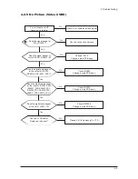

3 Alignments and Adjustments
3-5
No
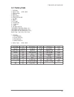
Item
1
2
3
4
5
6
7
8
9
10
11
12
13
TCD3 Contrast
TCD3 Brightness
TCD3 CR Saturation
TCD3 CB Saturation
TCD3 YC Delay
Analog Y offset
Analog PB offset
Analog PR offset
Analog Y Gain
Analog PB Gain
Analog PR Gain
Black Level Setting
Brightness(SVP)
0 ~ 255
0 ~ 255
0 ~ 255
0 ~ 255
0 ~ 15
00 ~ 255
00 ~ 255
00 ~ 255
00 ~ 255
00 ~ 255
00 ~ 255
00 ~ 255
0 ~ 255
AV Calibration(78h)
AV Calibration(20h)
78h
78h
00h
40h
80h
80h
D6h
FEh
FEh
78h
20h
78h
78h
00h
3
DVI Calibration(80h)
DVI Calibration(80h)
DVI Calibration(D6h)
FEh
FEh
78h
20h
78h
78h
00h
40h
80h
80h
D6h
FEh
FEh
78h
20h
78h
78h
00h
40h
80h
80h
D6h
FEh
FEh
EEPROM
Range
TV/AV/S-Video
Component
00h
00h
DVI/HDMI
PC
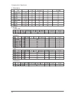
5) Picture Gain Adjust
No
Item
1
2
3
4
5
6
R-Offset
G-Offset
B-Offset
R-Gain
G-Gain
B-Gain
00 ~ 255
00 ~ 255
00 ~ 255
00 ~ 255
00 ~ 255
00 ~ 255
151(SC1 RGB)
151(SC1 RGB)
151(SC1 RGB)
123(SC1 RGB)
123(SC1 RGB)
123(SC1 RGB)
PC Calibration(128)
PC Calibration(128)
PC Calibration(128)
PC Calibration(192)
PC Calibration(192)
PC Calibration(192)
EEPROM
Range
TV/AV/S-Video
Component
X
X
DVI/HDMI
PC
5. MST9883
No
Item
1
2
3
4
5
6
7
8
9
10
FM-Prescale
NT-M-Prescale
SECAM-L-Prescale
NICAM-Prescale
AV-Prescale
12S_1 Prescale
12S_2 Prescale
Carrier Mute
Pilot High
Pilot Low
00 ~ 255
00 ~ 255
00 ~ 255
00 ~ 255
00 ~ 255
00 ~ 255
00 ~ 255
00 ~ 255
00 ~ 255
00 ~ 255
20h
20h
22h
42h
1Ah
10h
10h
42h
14
7
EEPROM
Range
PAL
6. MSP34XX/44XX
Summary of Contents for LE40M91B
Page 3: ...Contents ...
Page 4: ...Contents ...
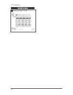
Page 27: ...4 Troubleshooting 4 4 WAVEFORMS 1 R G B Output Signal of IC500 ...
Page 29: ...4 Troubleshooting 4 6 2 Digital Output Data of IC500 3 Signal of HDMI Data ...
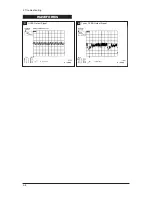
Page 31: ...4 Troubleshooting 4 8 WAVEFORMS 4 Tuner_CVBS Output Signal 3 CVBS Output Signal ...
Page 33: ...4 Troubleshooting 4 10 WAVEFORMS 4 CVBS Output Signal ...
Page 35: ...4 Troubleshooting 4 12 2 Digital Output Data of IC500 5 Analog Signal Y C to IC500 WAVEFORMS ...
Page 37: ...4 Troubleshooting 4 14 WAVEFORMS 6 The Signal are Inputed to IC1015 7 DC 12V ...
Page 69: ...8 1 8 Wiring Diagrams 8 Wiring Diagram 8 1 LE40M91BX Wiring Diagram ...
Page 70: ...8 Wiring Diagrams 8 2 8 2 Main Board Layout ...
Page 74: ...8 Wiring Diagrams 8 6 8 4 Power Board Layout ...
Page 77: ...8 9 8 Wiring Diagrams ...
Page 81: ...9 Schematic Diagrams 9 2 9 2 Input Output Schematic Diagram ...
Page 82: ...9 Schematic Diagrams 9 3 9 3 Input Output Schematic Diagram ...
Page 83: ...9 Schematic Diagrams 9 4 9 4 Micom Schematic Diagram ...
Page 84: ...9 Schematic Diagrams 9 5 9 5 SVP PX Schematic Diagram ...
Page 85: ...9 Schematic Diagrams 9 6 9 6 Application Schematic Diagram ...
Page 86: ...9 Schematic Diagrams 9 7 9 7 FRCH 100Hz LVDS Schematic Diagram ...
Page 87: ...9 Schematic Diagrams 9 8 Memo ...
Page 98: ...12 PCB Diagram 12 1 12 PCB Diagram 12 1 Main PCB Layout ...