


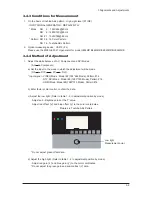


3 Alignments and Adjustments
3-1
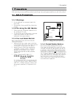
3 Alignments and Adjustments
3-1 Service Instruction
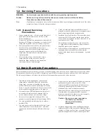
1. Usually, a color TV-VCR needs only slight touch-up adjustment upon installation.
Check the basic characteristics such as height, horizontal and vertical sync.
2. Use the specified test equipment or its equivalent.
3. Correct impedance matching is essential.
4. Avoid overload. Excessive signal from a sweep generator might overload the front-end
of the TV. When inserting signal markers, do not allow the marker generator to distort
test result.
5. Connect the TV only to an AC power source with voltage and frequency as specified on
the backcover nameplate.
6. Do not attempt to connect or disconnect any wire while the TV is turned on. Make sure
that the power cord is disconnected before replacing any parts.
7. To protect aganist shock hazard, use an isolation transform.
Summary of Contents for LE40M91B
Page 3: ...Contents ...
Page 4: ...Contents ...
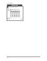
Page 27: ...4 Troubleshooting 4 4 WAVEFORMS 1 R G B Output Signal of IC500 ...
Page 29: ...4 Troubleshooting 4 6 2 Digital Output Data of IC500 3 Signal of HDMI Data ...
Page 31: ...4 Troubleshooting 4 8 WAVEFORMS 4 Tuner_CVBS Output Signal 3 CVBS Output Signal ...
Page 33: ...4 Troubleshooting 4 10 WAVEFORMS 4 CVBS Output Signal ...
Page 35: ...4 Troubleshooting 4 12 2 Digital Output Data of IC500 5 Analog Signal Y C to IC500 WAVEFORMS ...
Page 37: ...4 Troubleshooting 4 14 WAVEFORMS 6 The Signal are Inputed to IC1015 7 DC 12V ...
Page 69: ...8 1 8 Wiring Diagrams 8 Wiring Diagram 8 1 LE40M91BX Wiring Diagram ...
Page 70: ...8 Wiring Diagrams 8 2 8 2 Main Board Layout ...
Page 74: ...8 Wiring Diagrams 8 6 8 4 Power Board Layout ...
Page 77: ...8 9 8 Wiring Diagrams ...
Page 81: ...9 Schematic Diagrams 9 2 9 2 Input Output Schematic Diagram ...
Page 82: ...9 Schematic Diagrams 9 3 9 3 Input Output Schematic Diagram ...
Page 83: ...9 Schematic Diagrams 9 4 9 4 Micom Schematic Diagram ...
Page 84: ...9 Schematic Diagrams 9 5 9 5 SVP PX Schematic Diagram ...
Page 85: ...9 Schematic Diagrams 9 6 9 6 Application Schematic Diagram ...
Page 86: ...9 Schematic Diagrams 9 7 9 7 FRCH 100Hz LVDS Schematic Diagram ...
Page 87: ...9 Schematic Diagrams 9 8 Memo ...
Page 98: ...12 PCB Diagram 12 1 12 PCB Diagram 12 1 Main PCB Layout ...