2 Product Specifications
2-3
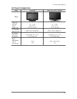
LE40M91BX
Model
Design
Frequency
Horizontal
Vertical
Display Color
30 ~ 61 kHz
100 ~ 120 Hz
16,777,216 colors
30 ~ 61 kHz
60 ~ 75 Hz
16,777,216 colors
PC Resolution
Maximum mode
Input Signal
Sync Signal
Video Signal
Power
Consumption
Normal
Power Saving
210W
< 2W
100W / 125W / 205W
< 1W
H/V Separate, TTL, P. or N.
0.7 Vp-p @ 75ohm
H/V Separate, TTL, P. or N.
0.7 Vp-p @ 75ohm
WXGA, 1360 x 768 @ 60 Hz
WXGA, 1360 x 768 @ 60 Hz
LE26R71B / LE32R71B / LE40R71B
2-3 Spec Comparison
Summary of Contents for LE40M91B
Page 3: ...Contents ...
Page 4: ...Contents ...
Page 27: ...4 Troubleshooting 4 4 WAVEFORMS 1 R G B Output Signal of IC500 ...
Page 29: ...4 Troubleshooting 4 6 2 Digital Output Data of IC500 3 Signal of HDMI Data ...
Page 31: ...4 Troubleshooting 4 8 WAVEFORMS 4 Tuner_CVBS Output Signal 3 CVBS Output Signal ...
Page 33: ...4 Troubleshooting 4 10 WAVEFORMS 4 CVBS Output Signal ...
Page 35: ...4 Troubleshooting 4 12 2 Digital Output Data of IC500 5 Analog Signal Y C to IC500 WAVEFORMS ...
Page 37: ...4 Troubleshooting 4 14 WAVEFORMS 6 The Signal are Inputed to IC1015 7 DC 12V ...
Page 69: ...8 1 8 Wiring Diagrams 8 Wiring Diagram 8 1 LE40M91BX Wiring Diagram ...
Page 70: ...8 Wiring Diagrams 8 2 8 2 Main Board Layout ...
Page 74: ...8 Wiring Diagrams 8 6 8 4 Power Board Layout ...
Page 77: ...8 9 8 Wiring Diagrams ...
Page 81: ...9 Schematic Diagrams 9 2 9 2 Input Output Schematic Diagram ...
Page 82: ...9 Schematic Diagrams 9 3 9 3 Input Output Schematic Diagram ...
Page 83: ...9 Schematic Diagrams 9 4 9 4 Micom Schematic Diagram ...
Page 84: ...9 Schematic Diagrams 9 5 9 5 SVP PX Schematic Diagram ...
Page 85: ...9 Schematic Diagrams 9 6 9 6 Application Schematic Diagram ...
Page 86: ...9 Schematic Diagrams 9 7 9 7 FRCH 100Hz LVDS Schematic Diagram ...
Page 87: ...9 Schematic Diagrams 9 8 Memo ...
Page 98: ...12 PCB Diagram 12 1 12 PCB Diagram 12 1 Main PCB Layout ...


