


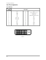

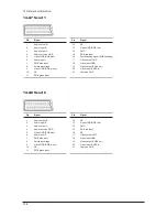


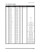

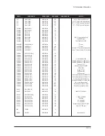
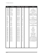

14 Reference Infomation
14-8
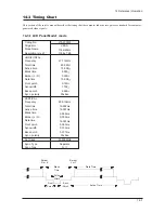
14-3-2 Supported Modes (1)
Timing No.
Originator
Mode Name
Resolution (H x V)
HORIZONTAL
Frequency
Total time
Active time
Blank time
Border (L / R)
Data time
Front porch
Sync.width
Back porch
Sync. polarity
VERTICAL
Frequency
Total time
Active time
Blank time
Border (L / R)
Data time
Front porch
Sync.width
Back porch
Sync. polarity
Dot Clock
28.322MHz
Sync. Type
Scan Type
Separate
N / I
31.169kHz
31.777
26.058
5.720
0.318
25.422
0.318
3.813
1.589
Negative
IBM
VGA2
720 x 400
2
70.087kHz
14.268ms
13.155ms
1.113ms
0.222ms
12.711ms
0.191ms
0.064ms
0.858ms
Positive
25.175MHz
Separate
N / I
31.469kHz
31.778
26.058
5.720
0.318
25.422
0.318
3.813
1.589
Negative
IBM
VGA3
640 x 480
3
59.940kHz
16.683ms
15.761ms
0.922ms
0.254ms
15.253ms
0.064ms
0.064ms
0.794ms
Negative
31.500MHz
Separate
N / I
37.861kHz
26.413
20.825
5.588
0.254
20.317
0.508
1.270
3.810
Negative
VESA
640/72Hz
720 x 400
11
72.809kHz
13.735ms
13.100ms
0.635ms
0.211ms
12.678ms
0.026ms
0.079ms
0.528ms
Negative
31.500MHz
Separate
N / I
37.500kHz
26.667
20.317
6.350
0.000
20.317
0.508
2.032
3.810
Negative
VESA
640/75Hz
720 x 400
17
75.000kHz
13.333ms
12.800ms
0.533ms
0.000ms
12.800ms
0.027ms
0.080ms
0.427ms
Negative
30.240MHz
Separate
N / I
37.000kHz
28.571
21.164
7.407
0.000
21.164
2.116
2.116
3.175
Negative
MAC
640/67Hz
640 x 480
32
66.667kHz
15.000ms
13.714ms
1.286ms
0.000ms
13.714ms
0.086ms
0.086ms
1.114ms
Negative
Summary of Contents for LE40M91B
Page 3: ...Contents ...
Page 4: ...Contents ...
Page 27: ...4 Troubleshooting 4 4 WAVEFORMS 1 R G B Output Signal of IC500 ...
Page 29: ...4 Troubleshooting 4 6 2 Digital Output Data of IC500 3 Signal of HDMI Data ...
Page 31: ...4 Troubleshooting 4 8 WAVEFORMS 4 Tuner_CVBS Output Signal 3 CVBS Output Signal ...
Page 33: ...4 Troubleshooting 4 10 WAVEFORMS 4 CVBS Output Signal ...
Page 35: ...4 Troubleshooting 4 12 2 Digital Output Data of IC500 5 Analog Signal Y C to IC500 WAVEFORMS ...
Page 37: ...4 Troubleshooting 4 14 WAVEFORMS 6 The Signal are Inputed to IC1015 7 DC 12V ...
Page 69: ...8 1 8 Wiring Diagrams 8 Wiring Diagram 8 1 LE40M91BX Wiring Diagram ...
Page 70: ...8 Wiring Diagrams 8 2 8 2 Main Board Layout ...
Page 74: ...8 Wiring Diagrams 8 6 8 4 Power Board Layout ...
Page 77: ...8 9 8 Wiring Diagrams ...
Page 81: ...9 Schematic Diagrams 9 2 9 2 Input Output Schematic Diagram ...
Page 82: ...9 Schematic Diagrams 9 3 9 3 Input Output Schematic Diagram ...
Page 83: ...9 Schematic Diagrams 9 4 9 4 Micom Schematic Diagram ...
Page 84: ...9 Schematic Diagrams 9 5 9 5 SVP PX Schematic Diagram ...
Page 85: ...9 Schematic Diagrams 9 6 9 6 Application Schematic Diagram ...
Page 86: ...9 Schematic Diagrams 9 7 9 7 FRCH 100Hz LVDS Schematic Diagram ...
Page 87: ...9 Schematic Diagrams 9 8 Memo ...
Page 98: ...12 PCB Diagram 12 1 12 PCB Diagram 12 1 Main PCB Layout ...