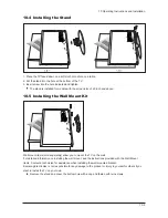


14 Reference Infomation
14-5
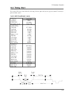
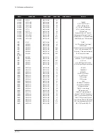
Both screen position and size will vary depending on the type of PC monitor and its resolution.
The resolutions in the table are recommended. (All resolutions between the supported limits are supported)
- The interlace mode is not supported.
- The set might operate abnormally if a non-standard video format is selected.
- DVI dose not support PC function.
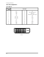
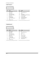
Pin
Separate
1
2
3
4
5
GND
Y
C
GND
GND
RCA Green
RCA Blue
RCA Red
RCA White
RCA Red
Y
GND
Pb (Cb)
GND
Pr (Cr)
GND
Audio L
GND
Audio R
GND
14-2-3 S-Video
Pin
Separate
1
2
3
4
5
6
7
8
9
10
11
12
13
14
15
Red
Green
Blue
GND
GND
GND Red
GND Green
GND Blue
DDC Input power(+5V)
IDENT PC
GND
DDC Data(SDA)
H SYNC
V SYNC
DDC Clock(SCL)
14-2-5 D-SUB
14-2-2 Component
RCA White
RCA Red
CVBS
Audio L
GND
Audio R
GND
14-2-4 A/V
RCA Yellow
14-2-6 PC Display mode
Mode
Resolution
Horizontal
Frequency(kHz)
640 x 480
720 x 400
640 x 480
640 x 480
800 x 600
800 x 600
800 x 600
1024 x 768
1024 x 768
1024 x 768
1360 x 768
31.469
31.469
37.864
37.500
37.879
48.077
46.875
48.364
56.476
60.023
47.712
59.940
70.087
72.809
75.000
60.317
72.188
75.000
60.000
70.069
75.029
60.015
31.500
31.500
40.000
50.000
49.500
65.000
75.000
78.750
85.800
- / -
- / -
+ / +
+ / +
+ / +
- / -
- / -
+ / +
+ / +
25.175
28.322
- / -
- / +
Vertical
Frequency(Hz)
Pixel Clock
Frequency(MHz)
Sync Polarity
(H/V)
IBM
VESA
Summary of Contents for LE40M91B
Page 3: ...Contents ...
Page 4: ...Contents ...
Page 27: ...4 Troubleshooting 4 4 WAVEFORMS 1 R G B Output Signal of IC500 ...
Page 29: ...4 Troubleshooting 4 6 2 Digital Output Data of IC500 3 Signal of HDMI Data ...
Page 31: ...4 Troubleshooting 4 8 WAVEFORMS 4 Tuner_CVBS Output Signal 3 CVBS Output Signal ...
Page 33: ...4 Troubleshooting 4 10 WAVEFORMS 4 CVBS Output Signal ...
Page 35: ...4 Troubleshooting 4 12 2 Digital Output Data of IC500 5 Analog Signal Y C to IC500 WAVEFORMS ...
Page 37: ...4 Troubleshooting 4 14 WAVEFORMS 6 The Signal are Inputed to IC1015 7 DC 12V ...
Page 69: ...8 1 8 Wiring Diagrams 8 Wiring Diagram 8 1 LE40M91BX Wiring Diagram ...
Page 70: ...8 Wiring Diagrams 8 2 8 2 Main Board Layout ...
Page 74: ...8 Wiring Diagrams 8 6 8 4 Power Board Layout ...
Page 77: ...8 9 8 Wiring Diagrams ...
Page 81: ...9 Schematic Diagrams 9 2 9 2 Input Output Schematic Diagram ...
Page 82: ...9 Schematic Diagrams 9 3 9 3 Input Output Schematic Diagram ...
Page 83: ...9 Schematic Diagrams 9 4 9 4 Micom Schematic Diagram ...
Page 84: ...9 Schematic Diagrams 9 5 9 5 SVP PX Schematic Diagram ...
Page 85: ...9 Schematic Diagrams 9 6 9 6 Application Schematic Diagram ...
Page 86: ...9 Schematic Diagrams 9 7 9 7 FRCH 100Hz LVDS Schematic Diagram ...
Page 87: ...9 Schematic Diagrams 9 8 Memo ...
Page 98: ...12 PCB Diagram 12 1 12 PCB Diagram 12 1 Main PCB Layout ...