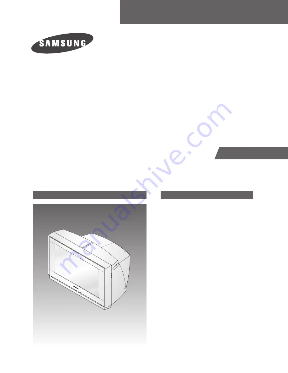
background image

COLOR TELEVISION RECEIVER

Chassis :  K55A(P) Youngstar_Rev.1

Model   :  CW29M066VGXXEC

CW29M066TGXXEC

COLOR TELEVISION RECEIVER

CONTENTS

Alignment and Adjustments

Exploded Views and Parts List

Electrical Parts List

PCB Diagrams 

Schematic Diagrams

1.

2.

3.

4.

5.

SERVICE

Manual

Summary of Contents for CW29M066VGXXEC

Page 1: ...is K55A P Youngstar_Rev 1 Model CW29M066VGXXEC CW29M066TGXXEC COLOR TELEVISION RECEIVER CONTENTS Alignment and Adjustments Exploded Views and Parts List Electrical Parts List PCB Diagrams Schematic Di...

Page 2: ...Electronics Co Ltd Mar 2004 Printed in Korea AA82 01386A This Service Manual is a property of Samsung Electronics Co Ltd Any unauthorized use of Manual can be punished under applicable International...

Page 3: ...50Hz 3 This service manual has been written on the basis of domestic remote control model adopting K55A chassis Depending on sales location and product specifications some of specifications herein may...

Page 4: ...GK so that the highest voltage becomes 160Vp p 1 1 4 White Balance Adjustment 1 Warm up the TV set for at least 30 minutes 2 Enter the Service Mode by pressing the remote control keys in the following...

Page 5: ...stments are correct 2 Adjust Screen Voltage before White Balance Adjustments Make sure Screen Voltage is correct 3 If White Balance has been readjusted re check Screen Voltage 4 After adjustments are...

Page 6: ...1 Set Colo r On Off item to 1 Ente r V ideo Adjust DN I e and ad just X 2 a nd Y 2 clo se to X1 an d Y 1 b y changing AD9883 R Offset Boffse t value 2 0 Y 1 2 0 At this time th e value read by W B me...

Page 7: ...ack Function LOW Remote Control Input Jack STAND BY Hight OFF LOW TIME ON H TIME OFF L DEGAUSSIGN COIL CONTROL Based on standard specifications H IN1 L IN2 BA7657F PIN 16 Control jack Reset active HIG...

Page 8: ...GNDHIGH OPEN STATUS Initially these pins select an input source at LOW state System NTSC PAL MUST be separated Active LOW 1080i control jack 1080i LOW RF Hight Magnetic field control PIN 36 37 38 39 4...

Page 9: ...4 43 13 7 9 4 5 49 36 36 31 29 27 40 32 34 21 24 7 9 9 3 1 33 30 34 25 33 30 40 REMARK Vertical AMP adj Gain Control Vertical Position adj DC bias adj Horizontal AMP adj Gain Control Horizontal Positi...

Page 10: ...al Linearity adj TOP adj Vertical Linearity adj Bottom adj Vertical S correction adj Horizontal pin distortion adj Horizontal pin distortion up adj Horizontal pin distortion low adj Horizontal Trapezi...

Page 11: ...adj Gain Control Vertical Position adj DC bias adj Horizontal AMP adj Gain Control Horizontal Position adj DC bias adj Vertical Linearity adj TOP Bottom adj Vertical Linearity adj TOP adj Vertical Lin...

Page 12: ...x H PAR UP COR LOW COR H TRA BOW ANGLE V POSI Fix CXA2151SUB01 CXA2151SUB02 REMARK Vertical AMP adj Gain Control Vertical Position adj DC bias adj Horizontal AMP adj Gain Control Horizontal Position a...

Page 13: ...PAR UP COR LOW COR H TRA BOW ANGLE V POSI Fix CXA2151SUB01 CXA2151SUB02 REMARK Vertical AMP adj Gain Control Vertical Position adj DC bias adj Horizontal AMP adj Gain Control Horizontal Position adj D...

Page 14: ...H PAR UP COR LOW COR H TRA BOW ANGLE V POSI Fix CXA2151SUB01 CXA2151SUB02 REMARK Vertical AMP adj Gain Control Vertical Position adj DC bias adj Horizontal AMP adj Gain Control Horizontal Position ad...

Page 15: ...LIN Fix LOW LIN Fix V SC Fix H PAR UP COR LOW COR H TRA BOW ANGLE V POSI Fix CXA2151SUB01 CXA2151SUB02 REMARK Vertical AMP adj Gain Control Vertical Position adj DC bias adj Horizontal AMP adj Gain Co...

Page 16: ...15 28 1 1 1 3 7 29 41 32 28 1 32 32 37 32 32 32 7 12 28 1 1 1 2 7 32 37 32 43 1 30 30 35 25 30 33 10 12 28 1 1 1 2 7 REMARK R cutoff control adj G cutoff control adj B cutoff control adj Initial Value...

Page 17: ...EMS R Cutoff G Cutoff B Cutoff Color on off CR offset CB offset R Drive G Drive B Drive Sub Bright Sub Contrast Sub Color Sub Tint CTI Level COL AXIS LTI Level VSU Merody Volume REMARK R cutoff contro...

Page 18: ...old voltage adj ABL IN PAL SETTING AGAIN VM OUT Level control VM OUT coring control VM f0 control VM Limit level control VM OUT phase control reference to R OUT Sharpness gain control color satuation...

Page 19: ...s gain control PAL SETTING AGAIN AKB Bch reference pulse time control PAL SETTING AGAIN VSP9407 Band High pass filter Peaking VSP9407 High pass filter 29 SDI 3 2 3 2 14 1 2 2 2 3 1 0 8 13 16 42 32 LG...

Page 20: ...2 3 1 1 8 29 SDI 20 7 15 28 1 1 1 2 2 2 3 1 1 8 32 LG 20 7 15 28 1 1 1 2 2 2 3 1 1 8 35 TSB 20 7 15 28 1 1 1 2 2 2 3 1 1 8 Australia Southeast Asia Hongkong S Asia ITEMS Sub Bright Sub Contrast Sub C...

Page 21: ...nt COL AXIS LTI Level VM Level VM Coring VM f0 VM Limit VM Delay SHP CD SHP f0 SHP f1 p o REMARK 29 SDI 38 7 15 28 1 1 1 2 2 2 3 1 1 8 32 LG 38 7 15 28 1 2 1 2 2 2 3 1 1 8 29 SDI 38 7 15 28 1 1 1 2 2...

Page 22: ...gain control SNI High pass filtering SNI Corring control SNI Clipping control SNI LPF DIF control VIDEO ADUJUST DNIe CIS ITEMS AD9883 R Gain AD9883 G Gain AD9883 B Gain AD9883 R Offset AD9883 G Offset...

Page 23: ...ping control SNI LPF DIF control VIDEO ADUJUST DNIe Australia Southeast Asia Hongkong S Asia Demo 20 10 30 3 30 9 On Off 20 8 30 3 30 9 DTV 20 10 20 3 15 1 ITEMS AD9883 R Gain AD9883 G Gain AD9883 B G...

Page 24: ...4 3 ON ON OFF ON OFF OFF Wide Wide CIS V DOLBY SCART ON 2 Tuner Russian ON OFF OFF OFF OFF ON Young star Hercules OFF ON V DOLBY SCART S ON OSD Language ON OFF OFF OFF ON Non Dome spk OFF OFF ON REMA...

Page 25: ...on 6th Remocon 32 29 29 A10 32 34 29 29 4 3 4 3 4 3 OFF ON Wide Wide V DOLBY RCA ON 2 Tuner West Europe ON OFF ON OFF ON OFF OFF ON ON ON Youngstar ON V DOLBY RCA ON 2 Tuner West Europe ON OFF ON OFF...

Page 26: ...DK YC DELAY P I YC DELAY P M YC DELAY P L YC DELAY S BG YC DELAY S DK YC DELAY S I YC DELAY S M YC DELAY S L YC DELAY N M YC DELAY YC Delay 29 1 5 2 0 2 1 0 0 6 9 9 0 0 0 32 1 5 2 0 2 1 0 0 6 9 9 0 0...

Page 27: ...50 50 40 50 40 45 50 50 76 184 255 255 255 255 0 124 125 29 0 0 1 2 6 7 70 50 50 50 50 50 57 50 50 45 50 50 43 50 50 40 50 50 76 186 255 255 255 255 0 124 125 32 0 0 1 2 5 7 80 50 50 50 50 50 52 50 50...

Page 28: ...255 102 28 28 28 28 147 153 0 48 255 255 255 255 3 5 3 0 0 0 0 0 0 0 0 0 32 248 80 71 8 70 255 102 255 102 28 28 28 28 147 153 0 48 255 255 255 255 3 7 5 0 0 0 0 0 0 0 0 0 REMARK V Saturation RGB DVD...

Page 29: ...0 71 Range 0 3 0 255 0 255 0 255 0 255 0 255 29 1 36 186 2 1 0 32 1 37 188 4 0 0 34 1 35 180 3 3 0 29 0 37 186 2 1 0 32 0 38 190 4 0 0 REMARK LTI Mode 1080i TTX V Position TTX H Position 16PIP UPPER C...

Page 30: ...6 7 100 50 50 60 50 50 70 50 50 50 50 50 50 50 50 45 50 50 76 186 32 255 32 184 0 124 125 32 LG 0 0 2 1 5 7 90 40 60 60 50 50 50 40 50 60 50 50 35 40 50 55 50 50 78 187 32 255 32 184 0 124 125 REMARK...

Page 31: ...119 1 32 LG 248 80 71 8 70 255 102 255 102 28 28 28 28 179 153 0 48 255 255 255 255 3 9 7 195 165 195 153 1 1 119 119 1 REMARK V Saturation RGB DVD 9407 Y Gian 9407 U Gian Luminance Delay 9407 V Gain...

Page 32: ...255 3 3 157 101 35 30 50 50 50 81 73 81 74 1 1 32 LG 1 35 186 4 0 0 235 255 3 3 157 101 35 30 50 50 50 81 73 81 74 1 1 REMARK LTI Mode 1080i TTX V Position TTX H Position 16PIP UPPER CORNER OFF SET 1...

Page 33: ...ctronics 1 31 1 5 Screen Change I2 C Bus Geometric Adjustment 12 Bow 4 V Linearity 5 Upper Linearity 11 H Trapezuim 3 H Shift 13 Angle 0 V Amp 9 Upper Coner 10 Low Coner 2 H EW 6 Low Linearity 7 V SC...

Page 34: ...Alignment and Adjustments 1 32 Samsung Electronics MEMO...

Page 35: ...POWER FJL6920YDTU N 200000MW TO 264 4 T0081 6003 000333 SCREW TAPTITE RH 2S M3 L10 ZPC YEL SW S N A 4 AA60 30001A WASHER PLATE M3 ID3 5 15X8 5 T1 0 SBHG S N A 4 AA62 00144A HEAT SINK KS3A K55A H OUT T...

Page 36: ...RBON 100OHM 5 1 8W AA TP 1 8X3 2MM 4 R125 2001 000281 R CARBON 100OHM 5 1 8W AA TP 1 8X3 2MM 4 R125 2001 000281 R CARBON 100OHM 5 1 8W AA TP 1 8X3 2MM 4 R125 2001 000281 R CARBON 100OHM 5 1 8W AA TP 1...

Page 37: ...7ohm 10 2W AF TP 3 9x10 4 R828 2008 001088 R FUSIBLE S 1ohm 5 2W AG TP 3 9x12mm 4 R304 2008 001088 R FUSIBLE S 1ohm 5 2W AG TP 3 9x12mm 4 R307 2008 001088 R FUSIBLE S 1ohm 5 2W AG TP 3 9x12mm 4 R425 2...

Page 38: ...4 L101 2701 000115 INDUCTOR AXIAL 10UH 10 3070 4 L102 2701 000159 INDUCTOR AXIAL 22UH 10 4298 4 L602 2701 000169 INDUCTOR AXIAL 3 9UH 10 2534 4 L608 2701 000180 INDUCTOR AXIAL 33UH 5 2534 4 L703 2701...

Page 39: ...ET ID1 5 OD2 L2 8 NI SN BSP3 1 2H S N A 4 EY819 6042 000002 EYELET ID1 5 OD2 L2 8 NI SN BSP3 1 2H S N A 4 EL408 6042 000001 EYELET ID2 2 OD2 7 L3 1 NI SN BSP3 1 S N A 4 EL801 6042 000001 EYELET ID2 2...

Page 40: ...4 5x 4 C2560 2301 000016 C FILM LEAD PEF 22nF 5 100V TP 7 2x4 5x 4 C2560 2301 000016 C FILM LEAD PEF 22nF 5 100V TP 7 2x4 5x 4 C2560 2301 000016 C FILM LEAD PEF 22nF 5 100V TP 7 2x4 5x 4 C526 2301 001...

Page 41: ...WC Z S N A 2 AA65 30110A CLAMPER CORE WIRE ALL MODEL NYLON 66 V2 S N A 2 qms HA83 00052A LP TAPE INK WIDTH 55 MM S N A 2 T0003 AA96 02033A ASSY C P FRONT 29M06 HIPS HB K55A SV 3 T0081 6003 001019 SCR...

Page 42: ...AN S N A 4 T0083 0402 000233 DIODE RECTIFIER FML G12S 200V 5A 4 T0083 0402 001230 DIODE RECTIFIER FMG G2CS 1000V 3A DO 41 4 T0087 1203 001006 IC POSI FIXED REG 78R05 TO 220F 4P PL 4 T0081 6003 000334...

Page 43: ...X3 2MM 4 R125 2001 000281 R CARBON 100OHM 5 1 8W AA TP 1 8X3 2MM 4 R125 2001 000281 R CARBON 100OHM 5 1 8W AA TP 1 8X3 2MM 4 R125 2001 000281 R CARBON 100OHM 5 1 8W AA TP 1 8X3 2MM 4 R125 2001 000281...

Page 44: ...8 R FUSIBLE S 1ohm 5 2W AG TP 3 9x12mm 4 R425 2008 001109 R FUSIBLE S 0 18ohm 10 2W AG TP 3 9x12 4 R424 2008 001109 R FUSIBLE S 0 18ohm 10 2W AG TP 3 9x12 4 R829 2008 001148 R FUSIBLE 3 3OHM 5 1W AG T...

Page 45: ...GP TP 5x11 5 4 C701 2401 003034 C AL 220uF 20 16V WT TP 8x11 5 5 4 C701 2401 003034 C AL 220uF 20 16V WT TP 8x11 5 5 4 C701 2401 003046 C AL 47uF 20 50V WT TP 6 3x11 2 5 4 C701 2401 003578 C AL 1000u...

Page 46: ...4 EY435 6042 000002 EYELET ID1 5 OD2 L2 8 NI SN BSP3 1 2H S N A 4 EY436 6042 000002 EYELET ID1 5 OD2 L2 8 NI SN BSP3 1 2H S N A 4 EY437 6042 000002 EYELET ID1 5 OD2 L2 8 NI SN BSP3 1 2H S N A 4 EY818...

Page 47: ...1 2W AA TP 2 4X6 4 4 R075 2001 001194 R CARBON S 82KOHM 5 1 2W AA TP 2 4X6 4 4 R525 2002 001006 R COMPOSITION 4 7KOHM 15 1 2W AA TP 3 7 4 R515 2002 001017 R COMPOSITION 1Kohm 10 1 2W AA TP 3 7x9 4 R5...

Page 48: ...SSY COVER FRONT 29M06 K55A S N A 2 T0081 6002 000515 SCREW TAPPING RH 2 M4 L15 ZPC WHT SWR 2 T0081 6002 000515 SCREW TAPPING RH 2 M4 L15 ZPC WHT SWR 2 T0081 6003 001268 SCREW TAPTITE TH B M4 L12 ZPC Y...

Page 49: ...5 ZPC BLK SWR 1 T0081 S N A 1 11 AA64 04011A KNOB CONTROL M06 HIPS HB SV012P ALL SEH 1 T0022 S N A 1 12 6003 001026 SCREW TAPTITE RH B M4 L15 ZPC BLK SWR 1 T0081 S N A 1 13 AA61 00813B SUPPORT CRT 25M...

Page 50: ...25 94 5 147 206 25 112 25 133 122 75 181 25 211 5 9 5 125 15 375 122 25 179 25 210 5 150 166 145 75 95 75 97 25 47 25 25 18 75 18 75 Loc LX801S LX802S MD201 NT802S PC801S PFC01S PT801S Q402 Q404 Q601...

Page 51: ...04 QF02 QF03 QF04 QF05 QF09 QF10 X 19 65 85 5 30 5 45 83 75 34 5 52 131 25 122 25 127 5 119 25 149 131 83 5 69 5 13 25 30 38 131 5 149 5 143 83 5 4 75 4 75 65 75 22 5 35 75 40 25 26 5 44 75 132 5 140...

Page 52: ...Diagrams Samsung Electronics 4 3 4 3 MICOM PCB Loc DM01 ICM01 ICM02 ICM03 ICM04 ICM05 ZM01 ZM02 ZM03 ZM05 ZM06 X 27 5 18 53 63 5 54 5 25 46 45 5 46 5 4 5 7 Y 24 5 60 20 14 5 61 5 38 5 39 5 49 5 62 17...

Page 53: ...75 53 61 25 61 25 61 25 29 25 63 63 18 32 75 48 25 48 25 18 5 61 5 57 25 46 75 57 75 54 15 34 31 25 31 25 46 25 46 25 16 75 16 5 55 25 88 75 Loc IC04 IC05 IC10 IC11 IC12 IC13 IC14 IC15 IC16 IC17 IC18...

Page 54: ...4 5 111 75 71 71 36 25 38 75 30 5 14 75 49 25 49 25 49 25 46 25 53 29 25 18 48 25 48 57 25 46 75 34 31 25 31 25 46 25 46 25 26 25 16 75 Loc TC02 TC03 TC04 TC05 TC06 TC08 TD01 TQ01 TQ02 TR01 TR02 TR03...

Page 55: ...5 Schematic Diagrams Samsung Electronics Schematic Diagrams 5 1 5 1 MAIN 1 This Document can not be used without Samsung s authorization TP01 TP02 TP09 TP10 TP05 TP11 TP03 TP04 TP07 TP08 TP06...

Page 56: ...Schematic Diagrams 5 2 Samsung Electronics 5 2 MAIN 2 This Document can not be used without Samsung s authorization...

Page 57: ...Samsung Electronics Schematic Diagrams 5 3 5 3 MAIN 3 This Document can not be used without Samsung s authorization...

Page 58: ...Schematic Diagrams 5 4 Samsung Electronics 5 4 MAIN 4 This Document can not be used without Samsung s authorization...

Page 59: ...ematic Diagrams 5 5 This Document can not be used without Samsung s authorization TP01 TP02 TP03 TP04 TP05 TP06 TP07 TP08 TP09 TP10 TP11 TP12 TP13 TP14 TP15 TP16 TP17 TP18 TP19 TP20 TP21 TP22 TP23 TP2...

Page 60: ...Schematic Diagrams 5 6 Samsung Electronics This Document can not be used without Samsung s authorization 5 5 MICOM...

Page 61: ...Samsung Electronics Schematic Diagrams 5 7 This Document can not be used without Samsung s authorization 5 6 CRT...

Page 62: ...Schematic Diagrams 5 8 Samsung Electronics This Document can not be used without Samsung s authorization 5 7 F BOX 1...

Page 63: ...Samsung Electronics Schematic Diagrams 5 9 This Document can not be used without Samsung s authorization 5 8 F BOX 2...

Page 64: ...Schematic Diagrams 5 10 Samsung Electronics This Document can not be used without Samsung s authorization 5 9 F BOX 3...

Page 65: ...Samsung Electronics Schematic Diagrams 5 11 This Document can not be used without Samsung s authorization 5 10 F BOX 4...

Page 66: ...Schematic Diagrams 5 12 Samsung Electronics This Document can not be used without Samsung s authorization 5 11 F BOX 5...

Page 67: ...Samsung Electronics Schematic Diagrams 5 13 This Document can not be used without Samsung s authorization 5 12 F BOX 6...

Page 68: ...Schematic Diagrams 5 14 Samsung Electronics This Document can not be used without Samsung s authorization 5 13 Touch pad...

Page 69: ...Samsung Electronics Schematic Diagrams 5 15 This Document can not be used without Samsung s authorization 5 14 WOOFER...

Page 70: ...Schematic Diagrams 5 16 Samsung Electronics This Document can not be used without Samsung s authorization 5 15 Double focus...

Page 71: ...Samsung Electronics Schematic Diagrams 5 17 This Document can not be used without Samsung s authorization 5 16 A V SIDE...

Page 72: ...Schematic Diagrams 5 18 Samsung Electronics This Document can not be used without Samsung s authorization 5 17 LED 5 18 CONTROL This Document can not be used without Samsung s authorization...

Reviews: