Specifications
Alignment and Adjustments
Exploded View and Parts List
Electrical Part List
PCB Diagrams
Schematic Diagrams
1.
2.
3.
4.
5.
6.
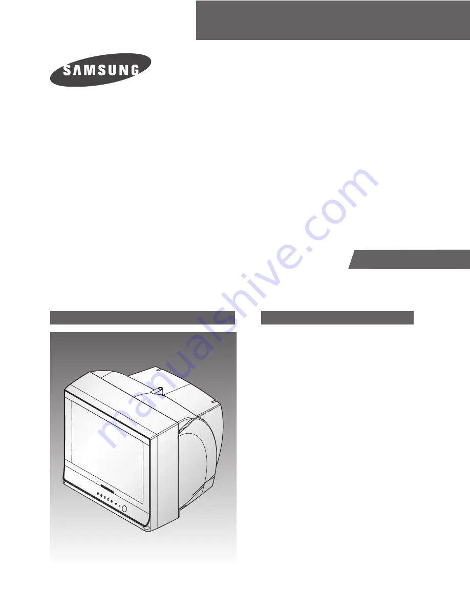
DIGITAL TELEVISION RECEIVER
Chassis :
KS9A(N)
Model
:
CL21N11MJZXXAX
SERVICE
Manual
COLOR TELEVISION RECEIVER
CONTENTS