


R&S FSP
Instrument Design and Function Description
1164.4556.82 3.3
E-1
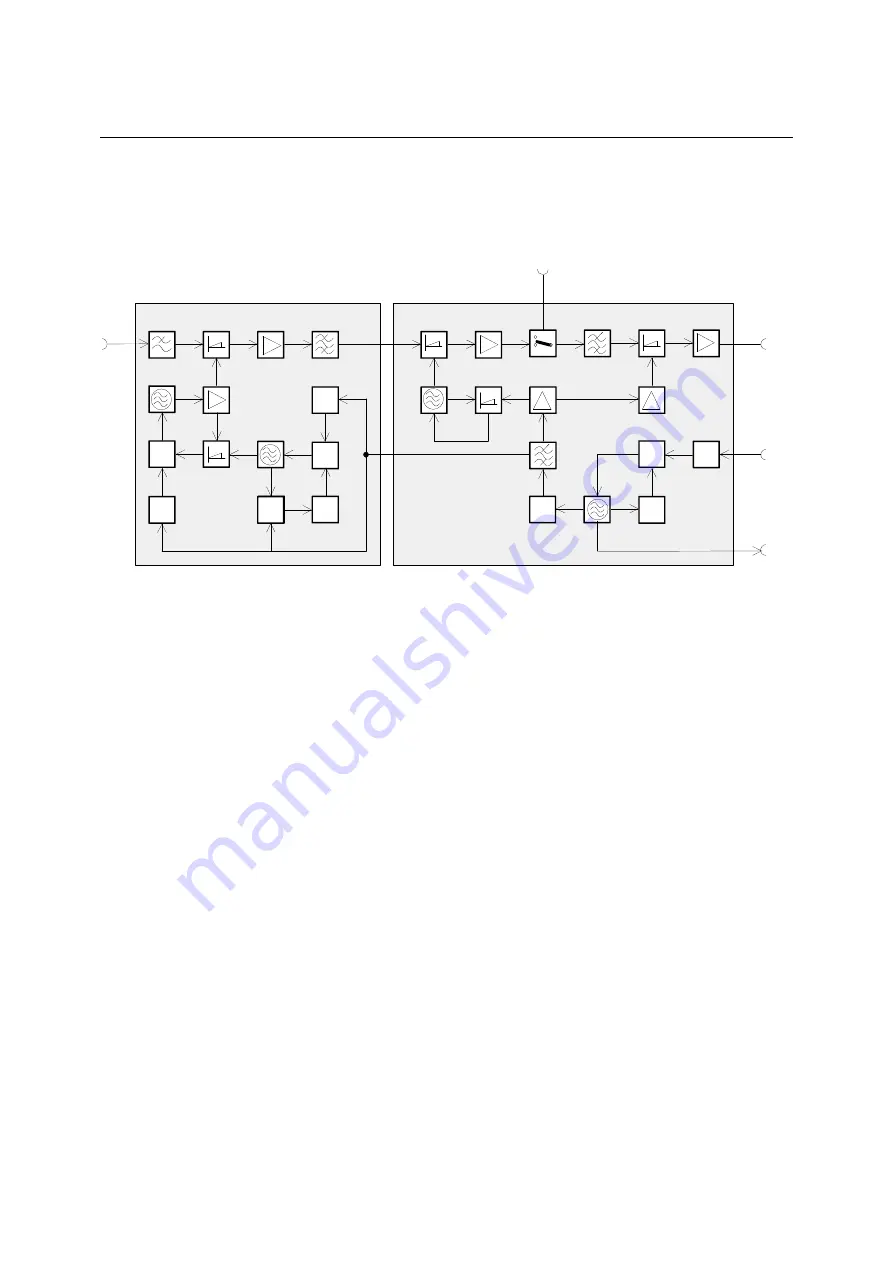
RF to IF Conversion for Frequencies < 3 GHz – Frontend
The frontend converts the receive frequencies in the range 9 kHz to 3 GHz to the low 20.4 MHz IF. The
frontend also includes the required local oscillators and associated frequency processing circuits. The
unit is made up of two PCBs accommodated in a common housing.
RF
Input
2nd IF
Input
IF Out
20.4 MHz
Sampling-
Mixer
PLL
1/N
1. IF
3476.4 MHz
PLL
1/N
PLL
*3
Frontend 1
Frontend 2
Ref.
384 MHz
Ref. In
10 MHz
Ref. Out
128 MHz
1/N
1/N
1/N
PLL
Fig. 3-2
RF-to-IF conversion for frequencies < 3 GHz
On frontend 1, the input signal in the range 0 to 3 GHz is converted to the first IF of 3476.4 MHz. The
input signal passes via the input lowpass to the first mixer. This lowpass at the mixer input provides for
suppression of the image frequency (image = LO + IF), such that the conversion remains unambiguous.
In the first mixer, the input signal is converted to an IF of 3476.4 MHz by means of the first LO (3476.4
to 6476.4 MHz). The mixer is followed by a low-noise IF amplifier, which compensates for the loss due
to mixing. The signal then passes a filter with a 3 dB bandwidth of approximately 100 MHz for filtering
the first intermediate frequency. The local oscillator frequency (3.4 to 6.6 GHz) required for this
conversion is also generated on this board. This signal is generated by three VCOs, which are
synchronized to a low phase noise VCO running from 320 to 352 MHz. The synchronization is done with
a sampling mixer; the resulting IF is variable. A signal with 384 MHz from frontend 2 is the reference
frequency The conversion gain of frontend 1 is approximately 0 dB.
Generation of the second and third local oscillator frequencies and conversion from the first to the third
IF are performed on frontend 2.
The module has 2 inputs for IF signals which can be selected using a changeover switch.
The signal from frontend 1 is converted to the second IF of 404.4 MHz in the second mixer. The signal
is then amplified, and the input switch for selection of the input signal is connected into the signal path.
The signal is routed to a 404.4 MHz filter with a 3 dB bandwidth of 10 MHz for further signal processing.
This filter functions as a resolution filter if the resolution bandwidth is set to 10 MHz, and it suppresses
the image frequency which might occur with the third conversion. The filter is followed by the third mixer,
which converts to 20.4 MHz. The conversion gain of frontend 2 is approximately 8 dB against the first IF
input and approximately 0 dB against the second IF input.
Located on frontend 2 is also the reference frequency generation for 128 MHz. This signal is generated
by a VTXO, which is synchronized to the 10 MHz reference applied from the IF filter. The third LO is
generated by multiplication of the oscillator signal (*3) and filtering of the comb line; this signal is also
used as a reference for frontend 1. The second LO for the second conversion is obtained using an
oscillator which is synchronized to a harmonic of the 384 MHz reference.
Summary of Contents for 1164.4391.03
Page 4: ......
Page 14: ......
Page 16: ......
Page 18: ......
Page 20: ......
Page 22: ......
Page 24: ......
Page 92: ...Contents Adjustment R S FSP 1164 4556 82 I 2 2 E 1 This page is left blank intentionally...
Page 103: ...R S FSP Contents Repair 1164 4556 82 I 3 3 E 1 This page is left blank intentionally...
Page 104: ......
Page 204: ...Contents Documents R S FSP 1164 4556 82 I 5 2 E 1 This page is left blank intentionally...
Page 208: ...Spare Parts R S FSP 1164 4556 82 5 4 E 2 This page is left blank intentionally...
Page 209: ...1164 4556 82 5 5 E 2 Spare Parts List Mechanical Drawings...
Page 222: ...List of R S FSP parts including spare parts R S FSP 1164 4556 82 5 18 E 2...
Page 223: ......
Page 224: ......
Page 225: ......
Page 226: ......
Page 227: ......
Page 228: ......
Page 229: ......
Page 230: ......
Page 231: ......
Page 232: ......
Page 233: ......
Page 234: ......
Page 235: ......
Page 236: ......
Page 237: ......
Page 238: ......
Page 239: ......
Page 240: ......
Page 241: ......
Page 242: ......
Page 243: ......
Page 244: ......
Page 245: ......
Page 246: ......
Page 247: ...11164 4556 82 5 19 E 2 Block Circuit Diagram...
Page 248: ......
Page 249: ......
Page 250: ......
Page 251: ......
Page 252: ......
Page 253: ......
Page 254: ......


