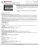
3.2.5 : VPX P4
The VPX P4 Control Plane is defined per VITA standard 46.9 which defines the signal mapping of XMC
1 (J16) differential user IO pins to VPX P4 (X12d+X8d) and VITA standard 46.6 which maps Gigabit
Ethernet to P4.
Pin
Row G
Row F
Row E
Row D
Row C
Row B
Row A
1
PWRDWN_L
GND
XMC_1_A5
XMC_1_B5
GND
XMC_1_D5
XMC_1_E5
2
GND
XMC_1_A7
XMC_1_B7
GND
XMC_1_D7
XMC_1_E7
GND
3
RST_IN_L
GND
XMC_1_A9
XMC_1_B9
GND
XMC_1_D9
XMC_1_E9
4
GND
XMC_1_A15
XMC_1_B15
GND
XMC_1_D15
XMC_1_E15
GND
5
NC
GND
XMC_1_A17
XMC_1_B17
GND
XMC_1_D17
XMC_1_E17
6
GND
XMC_1_A19
XMC_1_B19
GND
XMC_1_D19
XMC_1_E19
GND
7
NC
GND
XMC_1_A1
XMC_1_B1
GND
XMC_1_D1
XMC_1_E1
8
GND
XMC_1_A3
XMC_1_B3
GND
XMC_1_D3
XMC_1_E3
GND
9
NC
GND
XMC_1_A11
XMC_1_B11
GND
XMC_1_D11
XMC_1_E11
10
GND
XMC_1_A13
XMC_1_B13
GND
XMC_1_D13
XMC_1_E13
GND
11
NC
GND
P5_TXN
P5_TXP
GND
P5_RXN
P5_RXP
12
GND
P4_TXN
P4_TXP
GND
P4_RXN
P4_RXP
GND
13
NC
GND
LP1_DB_M
LP1_DB_P
GND
LP1_DA_M
LP1_DA_P
14
GND
LP1_DD_M
LP1_DD_P
GND
LP1_DC_M
LP1_DC_P
GND
15
NC
GND
LP0_DB_M
LP0_DB_P
GND
LP0_DA_M
LP0_DA_P
16
GND
LP0_DD_M
LP0_DD_P
GND
LP0_DC_M
LP0_DC_P
GND
Table 6 : VPX P4 Signals
XMC_1
VITA 46.9 X12d+X8d differential IO direct routing from XMC 1 J16 to VPX P4.
BLUE
VITA 46.6 Gigabit Ethernet Control Plane on VPX P4 routing.
PWRDWN_L
VP3500 Power down/up toggle. A LVTTL low-true input signal (pulled up on the VP3500) to power
control circuitry. A momentary switch to ground or pulling this signal low will toggle the VP3500 power on/
off circuitry.
RST_IN_L
Reset in. A LVTTL low-true input signal (pulled up on the VP3500) to the microcontroller used to reset
the VP3500. Depending on how this microcontroller setting is configured, this signal will reset the board
or the microcontroller will ignore it.
VP3500 User Manual • Document Number 101-3500-0001 • Revision A0
Property of Rigel Engineering, LLC. Confidential & Proprietary
690 Cone Park Court, Merritt Island, Florida 32952
page 36