R01UH0092EJ0110 Rev.1.10
Page 295 of 807
Jul 31, 2012
M16C/64C Group
17. Timer A
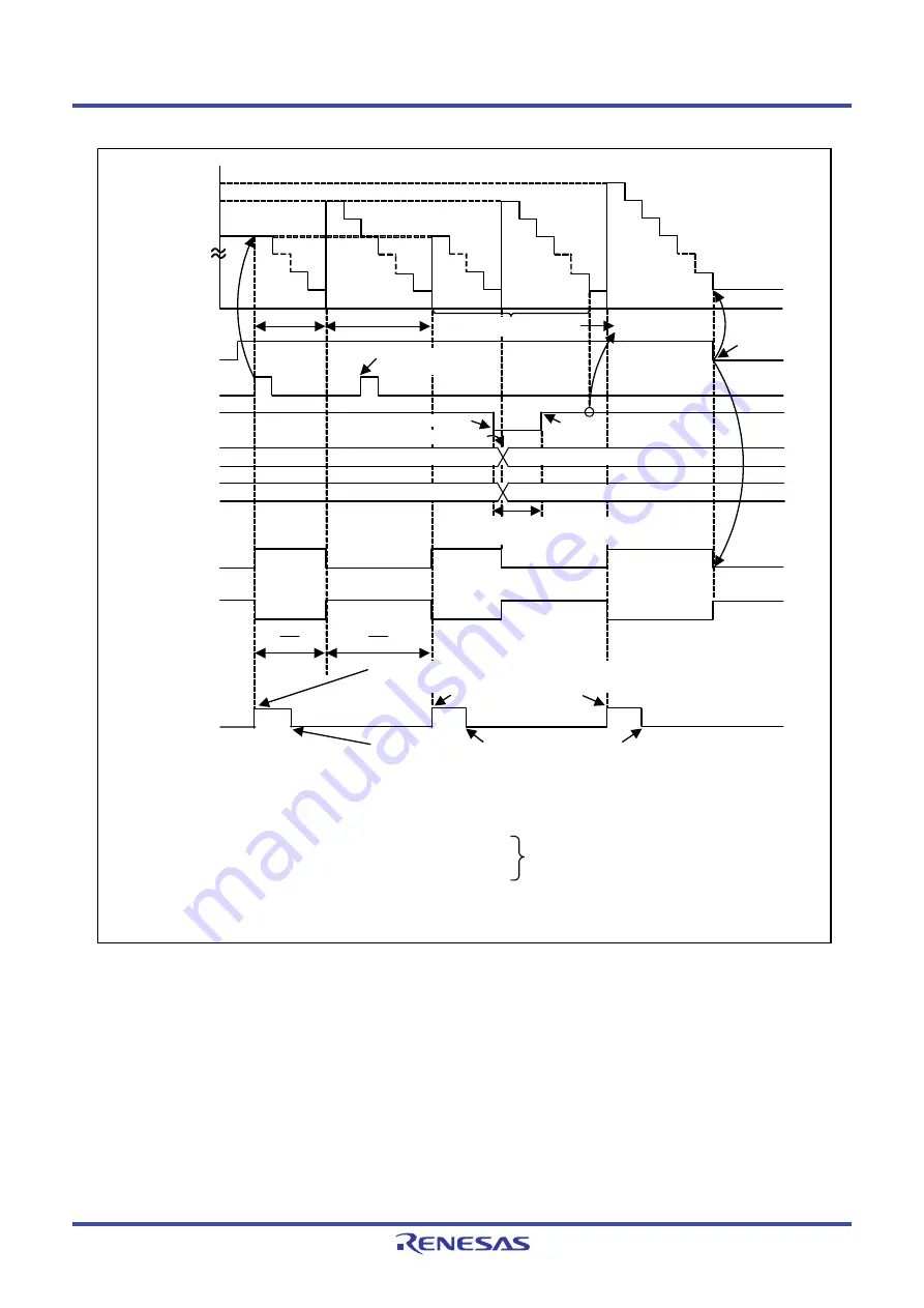
Figure 17.13 Operation Example in Programmable Output Mode
i = 1, 2, 4
The above timing diagram assumes the following:
- The MR0 bit in the TAiMR register
= 1 (pulse output)
- The MR1 bit in the TAiMR register
= 1
- The MR2 bit in the TAiMR register
= 1
- Bits TAiTGH to TAiTGL in the ONSF or TRGSR register = 00b
fj: Count source frequency
POFSi
: Bits in the TAPOFS register
TAiIN input
0000h
TAiOUT output
Low-level output
at count stop
IR bit
in the TAiIC register
TAiS bit
in the TABSR register
n1
Count stopped
Set to 0
by a program
Count stopped
m1
m1
fj
Set to 0 by accepting an interrupt request, or by a program.
The rising edge of the TAiIN pin input is the trigger.
Count started
Count the updated
value.
Cannot be a retrigger
after count start
Update registers TAi and
TAi1 during this period.
Interrupt request generated
- when TAiOUT changes state from low to high while POFSi is 0.
- when TAiOUT changes state from high to low while POFSi is 1.
POFSi = 0
POFSi = 1
m2
n1
m1
n1
fj
TAiOW bit
in the TAOW register
TAi register
TAi1 register
Do not change the output waveform during this period.
(When reloading, use the value before updated.)
m1
n1
m2
n2
Set to 1 by a program
Set to 0 by a program
Update a value by a program
Summary of Contents for M16C Series
Page 846: ...M16C 64C Group R01UH0092EJ0110...


