background image


                                                                                        UMTS/HSPA+  Module  Series


UC200A-GL_Hardware_Design                                                                                                                  53 / 79 


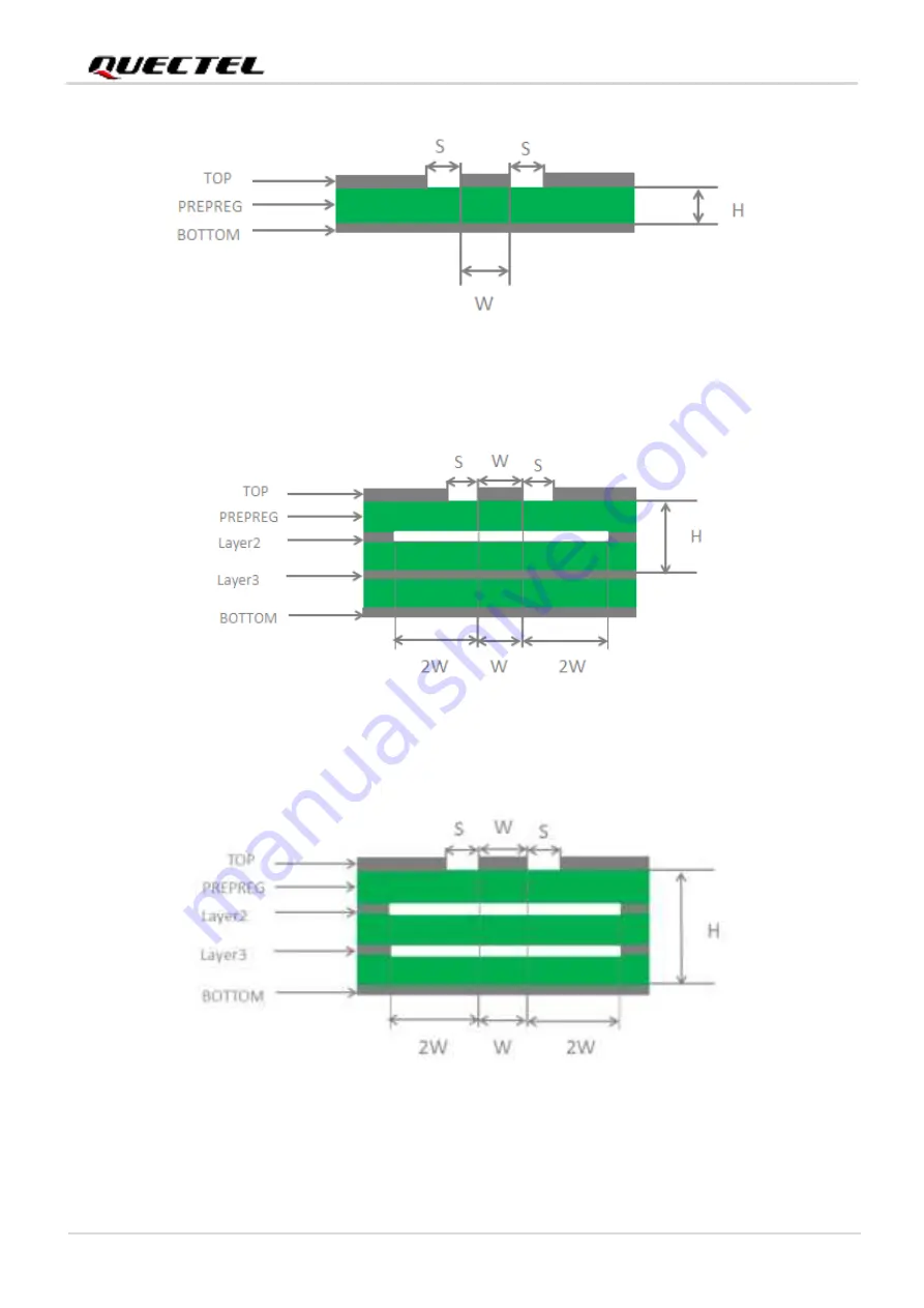
Figure 30:


Coplanar Waveguide Design on a 2-layer PCB 


Figure 31: Coplanar Waveguide Design on a 4-layer PCB (Layer 3 as Reference Ground) 


Figure 32: Coplanar Waveguide Design on a 4-layer PCB (Layer 4 as Reference Ground) 


Summary of Contents for UMTS Module Series

Page 1: ...UC200A GL Hardware Design UMTS HSPA Module Series Version 1 0 0 Date 2021 11 19 Status Preliminary...

Page 2: ...mploy commercially reasonable efforts to provide the best possible experience you hereby acknowledge and agree that this document and related services hereunder are provided to you on an as available...

Page 3: ...ool information or product We moreover disclaim any and all warranties arising from the course of dealing or usage of trade Disclaimer a We acknowledge no liability for any injury or damage arising fr...

Page 4: ...interference on sensitive medical equipment so please be aware of the restrictions on the use of wireless devices when in hospitals clinics or other healthcare facilities Cellular terminals or mobile...

Page 5: ...Series UC200A GL_Hardware_Design 4 78 About the Document Revision History Version Date Author Description 2021 10 29 Anthony LIU Ethan FANG Creation of the document 1 0 0 2021 10 29 Anthony LIU Ethan...

Page 6: ...B Application with USB Remote Wakeup Function 23 3 2 2 1 USB Application with USB Suspend Resume and MAIN_RI Wakeup Function 24 3 2 2 2 USB Application without USB Suspend Function 25 3 3 Airplane Mod...

Page 7: ...sign of RF Routing 52 5 3 Requirements for Antenna Design 54 5 4 RF Connector Recommendation 55 6 Electrical Characteristics Reliability 57 6 1 Absolute Maximum Ratings 57 6 2 Power Supply Ratings 58...

Page 8: ...4 Table 20 Pin Definition of ADC Interface 45 Table 21 Characteristics of ADC Interface 46 Table 22 Pin Definition of Indication Signal 46 Table 23 Working State of the Network Connection Status Activ...

Page 9: ...UMTS HSPA Module Series UC200A GL_Hardware_Design 8 78 Table 42 Terms and Abbreviations 72...

Page 10: ...r 38 Figure 21 Reference Circuit of U SIM Interface with a 6 pin U SIM Card Connector 39 Figure 22 Timing Sequence for Short frame mode 40 Figure 23 PCM and I2C Interface Circuit Reference Design 41 F...

Page 11: ...UMTS HSPA Module Series UC200A GL_Hardware_Design 10 78 Figure 43 Plastic Reel Dimension Drawing 70 Figure 44 Packaging Process 71...

Page 12: ...to design and set up mobile applications easily 1 1 Special Marks Table 1 Special Marks Mark Definition Unless otherwise specified when an asterisk is used after a function feature interface pin name...

Page 13: ...nd GPRS coverage Provides audio support for customers specific applications Table 2 Brief Introduction of the Module 2 1 Frequency Bands and Functions Table 3 Wireless Network Type Categories Packagin...

Page 14: ...orts master and slave modes I2C Interface Supports one digital I2C interface Complies with I2C bus protocol specifications 100 400 kHz The multi host mode is not supported USB Interface Compliant with...

Page 15: ...ss E2 27 dBm 3 dB EGSM900 8 PSK Class E2 27 dBm 3 dB DCS1800 8 PSK Class E2 26 dBm 3 dB PCS1900 8 PSK Class E2 26 dBm 3 dB WCDMA Class 3 24 dBm 1 3 dB UMTS Features Supports 3GPP R7 HSPA HSDPA HSUPA a...

Page 16: ..._DET 23 PCM_DIN 24 PCM_DOUT 25 PCM_SYN C 26 PCM_CL K 27 SD_SDI O _DAT A3 28 SD_SDI O _DAT A2 29 SD_SDI O _DAT A1 30 SD_SDI O _DAT A0 31 SD_SDI O _CL K 32 SD_SDI O _CMD 33 SD_SDI O _VDD 34 RES ERVED 35...

Page 17: ...ected to the ground network Type Description AI Analog Input AIO Analog Input Output DI Digital Input DO Digital Output DIO Digital Input Output OD Open Drain PI Power Input PO Power Output Power Supp...

Page 18: ...ics Comment STATUS 61 OD Indicate the module s operation status External pull to 1 8 V If unused keep it open NET_STATUS 6 DO Indicate the module s network activity status VOHmin 1 35 V VOLmax 0 45 V...

Page 19: ...0 45 V VOHmin 1 35 V 3 0 V U SIM VOLmax 0 45 V VOHmin 2 55 V USIM_RST 17 DO U SIM card reset USIM_DET 13 DI U SIM card hot plug detect VILmin 0 3 V VILmax 0 6 V VIHmin 1 2 V VIHmax 2 0 V 1 8 V power...

Page 20: ...ain UART data terminal ready MAIN_RXD 68 DI Main UART receive MAIN_TXD 67 DO Main UART transmit VOLmax 0 45 V VOHmin 1 35 V Debug UART Interface Pin Name Pin No I O Description DC Characteristics Comm...

Page 21: ...Interface Pin Name Pin No I O Description DC Characteristics Comment ANT_MAIN 49 AIO Main antenna interface ADC Interface Pin Name Pin No I O Description DC Characteristics Comment ADC0 45 AI General...

Page 22: ...S 232 converter cable earphone antenna and other peripherals to control or to test the module For more details see document 1 Pull up by default In low voltage level module can enter into airplane mod...

Page 23: ...data Talk Data Network connection is ongoing In this mode the power consumption is decided by network setting and data transfer rate Minimum Functionality Mode AT CFUN 0 can set the module to a minim...

Page 24: ...Figure 2 Sleep Mode Application via UART Driving MAIN_DTR to low level by host will wake up the module When the module has a URC to report the URC will trigger the behavior of MAIN_RI pin Please refe...

Page 25: ...remote wakeup signals via USB bus to wake up the host 3 2 2 1 USB Application with USB Suspend Resume and MAIN_RI Wakeup Function If the host supports USB Suspend Resume but does not support remote wa...

Page 26: ...refer to Chapter 4 9 for details about MAIN_RI behavior 3 2 2 2 USB Application without USB Suspend Function If the host does not support USB Suspend function please disconnect USB_VBUS with addition...

Page 27: ...g the pin to low level can make the module enter airplane mode 3 3 2 Software AT CFUN fun command provides choices of the functionality level through setting fun into 0 1 or 4 AT CFUN 0 minimum functi...

Page 28: ...eferred as the power supply The following figure shows a reference design for 5 V input power source The design uses the LDO MIC29302WU from Micrel company The typical output of the power supply is ab...

Page 29: ...e these capacitors close to the VBAT_BB and VBAT_RF pins The main power supply from an external application has to be a single voltage source and can be expanded to two sub paths with star structure T...

Page 30: ...f PWRKEY When the module is in power down mode it can be turned on to normal mode by driving the PWRKEY pin to a low level for at least 500 ms It is recommended to use an open drain collector driver t...

Page 31: ...rotection A reference circuit is shown in the following figure PWRKEY M odul e S1 Close to S1 TVS Turn on pulse Figure 10 Turning on the Module with a Button The power up scenario is illustrated in th...

Page 32: ...trated in the following figure Figure 12 Timing of Turning off Module 3 6 2 Turn off the Module with AT Command It is safe to use AT QPOWD to turn off the module which is equal to turn off the module...

Page 33: ...tor driver or button can be used to control the RESET_N Reset pulse RESET_N 4 7K 47K 300 ms Figure 13 Reference Circuit of RESET_N with Driving Circuit 1 To avoid damaging internal flash do not switch...

Page 34: ...ed in the following figure VIL 0 5 V VBAT Module Status Running RESET_N Baseband restart Baseband resetting 300 ms Figure 15 Timing of Resetting Module 1 Please ensure that there is no large capacitan...

Page 35: ...tware debugging and firmware upgrade The following table shows the pin definition of USB interface Table 11 Functions of the USB Interface Pin definition of the USB interface is here as follows Table...

Page 36: ...aced close to the module and R1 and R2 should be placed close to each other The extra stubs of trace must be as short as possible The following principles should be complied with when designing the US...

Page 37: ...de the module supports firmware upgrade over USB interface Table 13 Pin Definition of USB_BOOT Interface The following figure shows a reference circuit of USB_BOOT interface Module USB_BOOT VDD_EXT 4...

Page 38: ...able 14 Pin Definition of U SIM Interface 1 Please make sure that VBAT is stable before pulling down PWRKEY pin It is recommended that the time between powering up VBAT and pulling down PWRKEY pin is...

Page 39: ...nterface is as follows Module USIM_VDD USIM_GND USIM_RST USIM_CLK USIM_DATA USIM_DET 0R 0R 0R VDD_EXT 51K 100 nF GND GND 33 pF 33 pF 33 pF VCC RST CLK IO VPP GND GND USIM_VDD 15K U SIM Card Connector...

Page 40: ...s capacitor does not exceed 1 F Ensure the ground between the module and the U SIM card connector short and wide Keep the trace width of ground and USIM_VDD no less than 0 5 mm to maintain the same el...

Page 41: ...the MSB In this mode the PCM interface supports 256 kHz 512 kHz 1024 kHz 2048 kHz PCM_CLK at 8 kHz PCM_SYNC and also supports 4069 kHz PCM_CLK at 16 kHz PCM_SYNC The module supports a 16 bit linear en...

Page 42: ...8 V 4 7K 4 7K BCLK LRCK DAC ADC SCL SDA BIAS MICBIAS INP INN LOUTP LOUTN Codec 22R 33 pF 22R 22R 33 pF 22R 33 pF Figure 22 PCM and I2C Interface Circuit Reference Design PCM_DIN 24 DI PCM data input 1...

Page 43: ...n Definition of Debug UART Interface The module provides a 1 8 V UART interface A level translator should be used if the application is equipped with a 3 3 V UART interface A level translator TXS0108E...

Page 44: ...ansistor circuit is shown as below For the design of circuits shown in dotted lines please refer to that shown in solid lines but pay attention to the direction of connection MCU ARM TXD RXD VDD_EXT 1...

Page 45: ...M D2 C3 NM D3 C4 NM D4 C5 NM D5 C6 NM D6 C1 NM D1 C7 10 pF D7 C8 33 pF C9 100 nF C10 100 uF Figure 25 Reference Circuit of SD Card Interface In SD card interface design in order to ensure good communi...

Page 46: ...5 pF It is important to route the SDIO signal traces with ground surrounded The impedance of SDIO data trace is 50 10 Keep SDIO signals far away from other sensitive circuits signals such as RF circui...

Page 47: ...and NET_STATUS The following tables describe pin definition and logic level changes in different network status Name Min Typ Max Unit ADC0 Voltage Range 0 VBAT_BB V ADC1 Voltage Range 0 VBAT_BB V ADC...

Page 48: ...n LED indication circuit as below When the module is turned on normally the STATUS will present the low state Except for this the STATUS will present high impedance state The following figure shows di...

Page 49: ...RC can be outputted via UART port USB AT port and USB modem port which can be set by AT QURCCFG The default port is USB AT port In addition MAIN_RI behavior can be configured flexibly The MAIN_RI beha...

Page 50: ...able 26 Operating Frequency of UC200A GL Pin Name Pin No I O Description Comment ANT_MAIN 49 AIO Main antenna interface Only passive antennas are supported Considering authentication requirements it i...

Page 51: ...5 dB EGSM900 33 dBm 2 dB 5 dBm 5 dB DCS1800 30 dBm 2 dB 0 dBm 5 dB PCS1900 30 dBm 2 dB 0 dBm 5 dB GSM850 8 PSK 27 dBm 3 dB 5 dBm 5 dB GSM900 8 PSK 27 dBm 3 dB 5 dBm 5 dB DCS1800 8 PSK 26 dBm 3 dB 0 d...

Page 52: ...connection It is recommended to reserve a type matching circuit for better RF performance and the type matching components C1 R1 C2 should be placed as close to the antenna as possible The capacitors...

Page 53: ...led to 50 The impedance of the RF traces is usually determined by the trace width W the materials dielectric constant the height from the reference ground to the signal layer H and the spacing between...

Page 54: ...ardware_Design 53 79 Figure 30 Coplanar Waveguide Design on a 2 layer PCB Figure 31 Coplanar Waveguide Design on a 4 layer PCB Layer 3 as Reference Ground Figure 32 Coplanar Waveguide Design on a 4 la...

Page 55: ...nes There should be clearance under the signal pin of the antenna connector or solder joint The reference ground of RF traces should be complete Meanwhile ground vias around RF traces and the referenc...

Page 56: ...onnector is used for antenna connection it is recommended to use U FL R SMT connector provided by Hirose Figure 33 Dimensions of U FL R SMT Connector Unit mm U FL LP serial connectors listed in the fo...

Page 57: ...Module Series UC200A GL_Hardware_Design 56 79 The following figure describes the space factor of mated connector Figure 35 Space Factor of Mated Connector Unit mm For more details please visit http h...

Page 58: ...r power supply and voltage on digital and analog pins of the module are listed in the following table Table 30 Absolute Maximum Ratings Parameter Min Max Unit VBAT_RF VBAT_BB 0 3 5 5 V USB_VBUS 0 3 5...

Page 59: ...burst Maximum power control level at EGSM 900 0 0 400 mV IVBAT Peak supply current during transmission slot Maximum power control level at EGSM 900 0 1 8 2 0 A USB_VBUS USB connection detection 3 0 5...

Page 60: ...ected TBD mA WCDMA PF 64 USB connected TBD mA GPRS data transfer EGSM900 4DL 1UL 32 34 dBm TBD mA EGSM900 3DL 2UL 32 31 dBm TBD mA EGSM900 2DL 3UL 31 08 dBm TBD mA EGSM900 1DL 4UL 29 28 dBm TBD mA DCS...

Page 61: ...20 02 dBm TBD mA WCDMA B8 HSUPA 21 03 dBm TBD mA GSM voice call EGSM900 PCL 5 32 24 dBm TBD mA EGSM900 PCL 12 19 09 dBm TBD mA EGSM900 PCL 19 5 82 dBm TBD mA DCS1800 PCL 0 29 40 dBm TBD mA DCS1800 PCL...

Page 62: ...on assembly and testing of the module adding ESD protective components to the ESD sensitive interfaces and points in the product design ESD characteristics of the module s pins are as follows Paramete...

Page 63: ...ch as voice SMS data transmission etc without any unrecoverable malfunction Radio spectrum and radio network are not influenced while one or more specifications such as Pout may exceed the specified t...

Page 64: ...al Information This chapter describes the mechanical dimensions of the module All dimensions are measured in millimeter mm and the dimensional tolerances are 0 2 mm unless otherwise specified 7 1 Mech...

Page 65: ...UMTS HSPA Module Series UC200A GL_Hardware_Design 64 79 Figure 37 Module Bottom Dimensions View Unit mm The package warpage level of the module conforms to the JEITA ED 7306 standard NOTE Pin 1...

Page 66: ..._Hardware_Design 65 79 7 2 Recommended Footprint Figure 38 Recommended Footprint Bottom View Keep at least 3 mm between the module and other components on the motherboard to improve soldering quality...

Page 67: ...66 79 7 3 Top and Bottom Views Figure 39 Top and Bottom View of the Module Images above are for illustration purpose only and may differ from the actual module For authentic appearance and label plea...

Page 68: ...han 10 e g a drying cabinet 4 The module should be pre baked to avoid blistering cracks and inner layer separation in PCB under the following circumstances The module is not stored in Recommended Stor...

Page 69: ...y after reflow soldering for the other side of PCB has been completed The recommended reflow soldering thermal profile lead free reflow soldering and related parameters are shown below Temp C Reflow Z...

Page 70: ...hite rust may be found 3 If a conformal coating is necessary for the module do NOT use any coating material that may chemically react with the PCB or shielding cover and prevent the coating material f...

Page 71: ...rriers One reel is 11 88 meters long and contains 250 modules The figures below show the package details measured in mm Figure 41 Carrier Tape Dimension Drawing Table 39 Carrier Tape Dimension Table U...

Page 72: ...aled carrier tape to the plastic reel and use the protective tape for protection 1 plastic reel can load 250 modules Place the packaged plastic reel humidity indicator card and desiccant bag into a va...

Page 73: ...l 3 Quectel_RF_Layout_Application_Note 4 Quectel_Module_Secondary_SMT_Application_Note Abbreviation Description ADC Analog to Digital Converter AMR WB Adaptive Multi Rate Wideband AON Active Optical N...

Page 74: ...Ready EFR Enhanced Full Rate ESD Electrostatic Discharge FDD Frequency Division Duplex FEM Front End Module FR Full Rate GLONASS Global Navigation Satellite System Russia GMSK Gaussian Minimum Shift...

Page 75: ...Grid Array LMHB Low Middle High Band LNA Low Noise Amplifier LTE Long Term Evolution MAC Media Access Control MB Middle Band MCU Microcontroller Unit MDC Management Data Clock MDIO Management Data Inp...

Page 76: ...ntegrated Circuit PRX Primary Receive QAM Quadrature Amplitude Modulation QPSK Quadrature Phase Shift Keying QZSS Quasi Zenith Satellite System RI Ring Indicator RF Radio Frequency RGMII Reduced Gigab...

Page 77: ...ile Telecommunications System URC Unsolicited Result Code USB Universal Serial Bus U SIM Universal Subscriber Identity Module VBAT Voltage at Battery Pin Vmax Maximum Voltage Vnom Nominal Voltage Vmin...

Page 78: ...nfigurations with respect to Part 2 1093 and different antenna configurations 4 For FCC Part 15 31 h and k The host manufacturer is responsible for additional testing to verify compliance as a composi...

Page 79: ...on the outside of the final device that contains the following text Contains FCC ID XMR202112UC200AGL The FCC ID can be used only when all FCC compliance requirements are met In the event that these...

Page 80: ...nt off and on the user is encouraged to try to correct the interference by one of the following measures Reorient or relocate the receiving antenna Increase the separation between the equipment and re...

Reviews: