Smart Module Series
SC690A_Series_Hardware_Design 46 / 105
Module
USB Type-C
USB_VBUS
R1
USB_HS_DP
USB_HS_DM
USB_CC1
USB_CC2
SS_DIR_OUT
SS_DIR_IN
USB_SS1_RX_P
VBUS
USB_SS1_RX_M
USB_SS2_RX_P
USB_SS2_RX_M
USB_SS1_TX_P
USB_SS1_TX_M
USB_SS2_TX_M
USB_SS2_TX_P
OPTION
D+
D-
CC1
CC2
RX1+
RX1-
TX1+
TX1-
RX2+
RX2-
TX2+
TX2-
GND
C8
C7
C6
C5
C4
C3
C1
C2
R2
R3
NM_10 K
0 R
NM_1 K
330 nF
330 nF
220 nF
220 nF
330 nF
220 nF
220 nF
330 nF
220 K
220 K
220 K
220 K
R4
R5
R6
R7
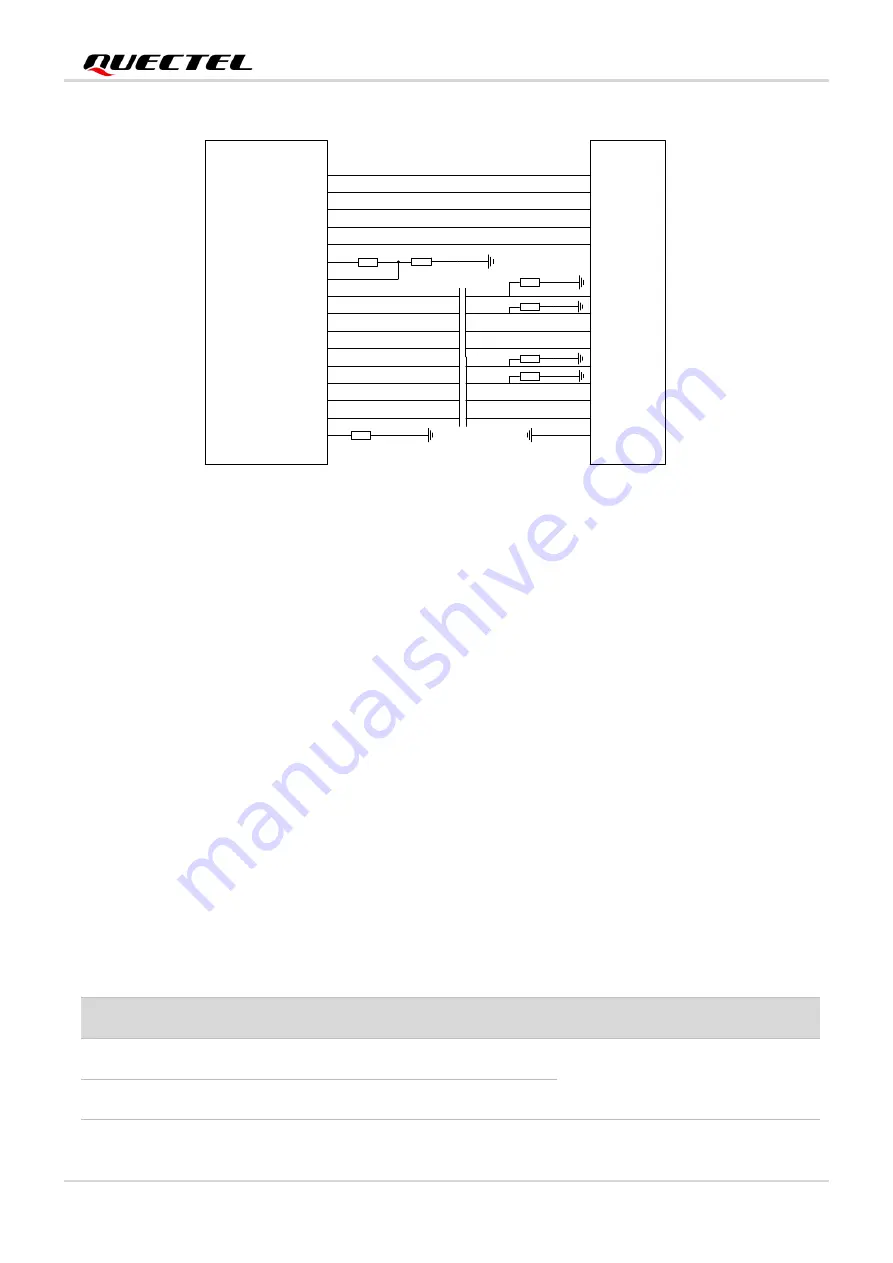
Figure 12: USB Type-C Interface Reference Design
To ensure USB performance, please comply with the following principles while designing USB interface.
⚫
It is important to route the USB signal traces as differential pairs with total grounding. The
impedance of USB differential trace is 90
Ω.
⚫
Pay attention to the influence of junction capacitance of ESD protection devices on USB data traces.
Typically, the capacitance value should be less than 2 pF for USB 2.0 and less than 0.5 pF for USB
3.1 Gen1.
⚫
Do not route signal traces under crystals, oscillators, magnetic devices, and RF signal traces. It is
important to route the USB differential traces in inner-layer with ground shielding on not only upper
and lower layers but also right and left sides.
⚫
Keep the ESD protection devices as close as possible to the USB connector.
⚫
Ensure the trace length difference between USB_DM
/
DP and that between USB 3.1 Gen1 RX/TX
differential pairs do not exceed 0.7 mm.
⚫
If micro USB is supported, R1 = NM, R2 = 10 K, R3 = 1 K. If USB Type-C is supported, R2/R3 = NM,
R1 = 0 R.
Table 12: USB Trace Length Inside the Module
Pin No.
Signal
Length (mm)
Length Difference (DP-DM)
33
USB_DM
38.16
-0.22
32
USB_DP
38.38


