Smart LTE Module Series
SC66 Hardware Design
SC66_Hardware_Design 64 / 139
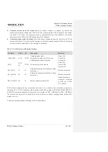
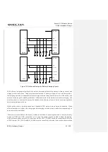
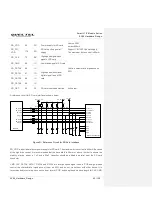
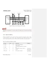
DATA0, DATA1, DATA2 and DATA3. CLK needs separate ground shielding.
Layout guidelines:
Control impedance to 50Ω±10%, and ground shielding is required.
The difference in trace lengths among the clock, data, and command signals should be less than 2
mm.
The bus length should be less than 50mm.
The spacing between signal lines should be 1.5 times the line width.
The capacitive reactance of data signal line should be < 8 pF.
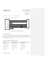
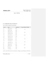
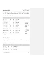
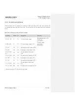
Table 19: SD Card Signal Trace Length Inside the Module
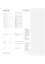
3.13. GPIO Interfaces
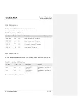
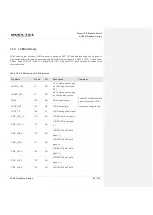
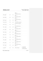
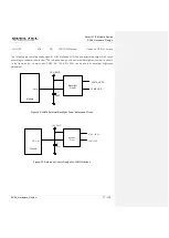
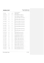
SC66 has abundant GPIO interfaces with power domain of 1.8V. The pin definition is listed below.
Table 20: Pin Definition of GPIO Interfaces
Pin No.
Signal
Length (mm)
70
SD_CLK
24.35
69
SD_CMD
24.30
68
SD_DATA0
24.30
67
SD_DATA1
24.30
66
SD_DATA2
24.25
65
SD_DATA3
24.30
Pin Name
Pin No.
GPIO
Default Status
Comment
GPIO_21
231
GPIO_21
B-PD:nppukp
1)
Wakeup
2)
GPIO_34
236
GPIO_34
B-PD:nppukp
GPIO_40
238
GPIO_40
B-PD:nppukp
Wakeup

