UMTS/HSPA+/LTE Standard Module Series
Mini PCIe-C EVB User Guide
Mini_PCIe-C_EVB_User_Guide 24 / 39
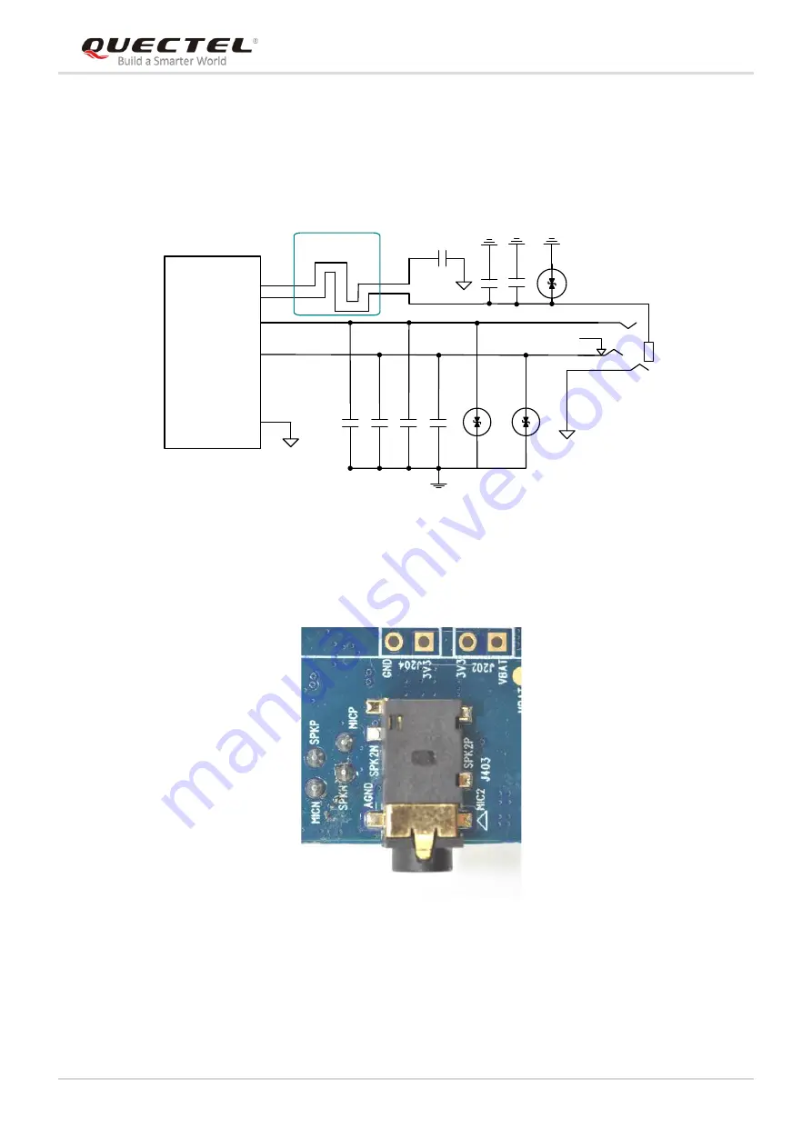
4.3.2.2. Earphone Interface (J403)
The analog audio interface J403 is designed for CTIA earphone. Its reference circuit design is shown as
below.
33pF
GND GND
Differential
layout
10pF
10pF 33pF
GND
GND
4.7uF
AGND
ESD
ESD
10pF
33pF ESD
J403
Audio Jack
2
4
5
3
1
AGND
AGND
J101
MICN
3
1
7
5
MICP
SPKN
SPKP
Figure 18: Reference Circuit Design for Earphone Interface J403
The figure and table below illustrate the pin assignment and pin definition of the earphone interface J403.
6
4
2
5
3
1
Figure 19: Pin Assignments of Earphone Interface J403


