


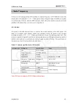


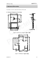


L50 Hardware Design
L50_HD_V1.0 -20-
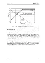
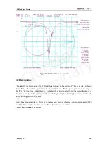
Figure 6: Seiko XH414 charging and discharging characteristics
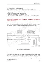
3.6 Timing Sequence
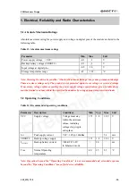
The ON_OFF pin is used to switch the module between full-on mode and hibernate mode.
L50 integrates power on reset circuit internally and external RESET signal which belongs to VIO/RTC
domain. When VCC and VIO/RTC are supplied simultaneously, the internal power on reset circuit
executes. Normally, external control of RESET is not necessary. When power supply VCC is removed
abruptly, an external RESET is suggested. Additionally, make sure the external RESET pin is pulled
up to VCC via a 10K resistor.
The following diagram is the reference timing sequence. Firstly, VCC and VIO/RTC power on ,then a
pulse of wakeup will be generated , after that when ON/OFF is toggled ,the module will go into the
full on mode and the WAKEUP will turn to high level. Next toggling of the ON/OFF will make the
module return to the hibernate mode. The state conversion is shown in the following figure.
Quectel
Preliminary