


LTE Module Series
EC21 Hardware Design
EC21_Hardware_Design Confidential / Released 47 / 94
PCM_CLK
27
IO
PCM data bit clock
1.8V power domain
I2C_SCL
41
OD
I2C serial clock
Require external pull-up to 1.8V
I2C_SDA
42
OD
I2C serial data
Require external pull-up to 1.8V
Clock and mode can be configured by AT command, and the default configuration is master mode using
short frame synchronization format with 2048kHz PCM_CLK and 8kHz PCM_SYNC. Please refer to
document [2]
about
AT+QDAI
command for details.
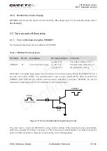
The following figure shows a reference design of PCM interface with external codec IC.
PCM_IN
PCM_OUT
PCM_SYNC
PCM_CLK
I2C_SCL
I2C_SDA
Module
1.8V
4
.7
K
4
.7
K
BCLK
LRCK
DAC
ADC
SCL
SDA
B
IA
S
MICBIAS
INP
INN
LOUTP
LOUTN
Codec
Figure 24: Reference Circuit of PCM Application with Audio Codec
1.
“*” means under development.
2. It is recommended to reserve RC (R=22 ohm, C=22pF) circuit on the PCM lines, especially for
PCM_CLK.
3. EC21 works as a master device pertaining to I2C interface.
NOTES
Quectel
Confidential


