background image

Chapter  3  Hardware  Configuration 


SP-6150/6155 SERIES USER MANUAL


Page: 3-8


3.4  HOW TO SET JUMPERS 

You  can  configure  your  board  by  setting  the  jumpers.  A  jumper  consists  of  two  or 
three  metal  pins  with  a  plastic  base  mounted  on  the  card.  By  using  a  small  plastic 

"

cap

"

,  also  known  as  the  jumper  cap  (with  a  metal  contact  inside),  you  are  able  to 

connect  the  pins.    So  you  can  configure  your  hardware  settings  by 

"

opening

"

  or 

"

closing

"

 jumpers. 

Jumpers can be combined into sets that  are  called jumper blocks. When jumpers are 
all in the block, you have to put them together to set up the hardware configuration. 
The figure below shows what this looks like. 

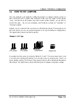
Jumpers & Caps 

If a jumper has three pins, for example, labeled 1, 2 and 3. You can connect pins 1 and 
2  to  create  one  setting  and  shorting.  You  can  also  select  to  connect  pins  2  and  3  to 
create another setting. The format of the jumper picture will be illustrated throughout 
this manual. The figure below shows different types of jumpers and jumper settings. 

Summary of Contents for SP-6150

Page 1: ...USER MANUAL SP 6150 6155 10 4 15 Fanless Panel PC Powered by Intel AtomTM Pentium Celeron CPU Processor SP 6150 SP 6155 M2...

Page 2: ...ronic or mechanical including photocopying and recording DISCLAIMER This user s manual is meant to assist users in installing and setting up the system The information contained in this document is su...

Page 3: ...ference at his own expense You are cautioned that any change or modifications to the equipment not expressly approve by the party responsible for compliance could void your authority to operate such e...

Page 4: ...O Ports Diagram 3 2 3 2 JUMPER CONNECTOR QUICK REFERENCE TABLE 3 3 3 3 COMPONENT LOCATIONS OF SYSTEM MAIN BOARD 3 5 3 3 1 Top View of System Main Board 3 5 3 3 2 Bottom View of System Main Board 3 7 3...

Page 5: ...ial ATA SATA SLOT 3 27 3 5 20 Serial ATA SATA 3 0 Connector 3 28 3 5 21 HDD Power Connector 3 28 3 5 22 AT ATX Mode Selection 3 29 3 5 23 TPM Module Selection 3 29 3 5 24 Slide Switch For LVDS Resolut...

Page 6: ...Touch Panel Connector 3 45 3 8 6 LED1 Connector 3 46 3 8 7 Touch Panel Up Signal Setting 3 47 3 8 8 Touch Panel Low Signal Setting 3 48 4 Software Utilities 4 1 4 1 Introduction 4 2 4 2 Installing Int...

Page 7: ...6 Watchdog Configuration 5 12 5 4 4 Advanced CPU Configuration 5 13 5 4 4 1 Advanced CPU Configuration Socket 0 CPU Information 5 14 5 4 4 2 Advanced CPU Configuration CPU Power Management 5 16 5 4 5...

Page 8: ...d Diagram A 5 SP 6150 Box Exploded Diagram A 6 SP 6155 Touch Panel Exploded Diagram A 7 SP 6155 LCD Display Exploded Diagram A 8 SP 6155 Panel Mount Exploded Diagram A 10 SP 6150 SP 6155 Button Cover...

Page 9: ...vi Flash BIOS Update B 25...

Page 10: ...nual is described below Version No Revision History Page No Date M1 Initial Release 2017 9 M2 Modify LCD Specification for SP 6150 Change rear I O ports diagram Change SP 6155 LCD display exploded Dia...

Page 11: ...55 SERIES USER MANUAL Page 1 1 1 Introduction This chapter provides the introduction for the SP 6150 SP 6155 system as well as the framework of the user manual The following topic is included About Th...

Page 12: ...ecifications and illustrates the physical appearances for the SP 6150 SP 6155 system Read the safety reminders carefully on how to take care of your system properly Chapter 3 System Configuration This...

Page 13: ...he SP 6150 SP 6155 system It describes how to set up the system quickly and outlines the system specifications The following topics are included Package List System Overview System Specification Safet...

Page 14: ...R MANUAL Page 2 2 2 1 Package List If you discover any of the items listed below are damaged or lost please contact your local distributor immediately Item Q ty SP 6150 SP 6155 1 Manual Driver DVD 1 Q...

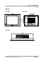
Page 15: ...Chapter 2 Getting Started SP 6150 6155 SERIES USER MANUAL Page 2 3 2 2 System Overview Unit mm SP 6150 Front View Rear View Top View 228 8 88 8 100 45 2 100 ANT2 ANT3 ANT4 SD SIM1 SIM2 ANT1 217 5...

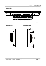
Page 16: ...Chapter 2 Getting Started SP 6150 6155 SERIES USER MANUAL Page 2 4 Bottom View Unit mm Left Side View Right Side View 78 10 12 4 202 8 140 6 31...

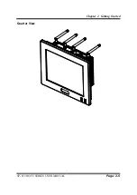
Page 17: ...Chapter 2 Getting Started SP 6150 6155 SERIES USER MANUAL Page 2 5 Quarter View...

Page 18: ...Chapter 2 Getting Started SP 6150 6155 SERIES USER MANUAL Page 2 6 Unit mm SP 6155 Front View Rear View Top View 371 217 5 ANT2 ANT3 ANT4 SD SIM1 SIM2 C L 100 VESA 100 VESA 94 7 408 308...

Page 19: ...Chapter 2 Getting Started SP 6150 6155 SERIES USER MANUAL Page 2 7 Bottom View Unit mm Left Side View Right Side View 93 46 10 10 2 268 230 20...

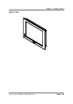
Page 20: ...Chapter 2 Getting Started SP 6150 6155 SERIES USER MANUAL Page 2 8 Quarter View...

Page 21: ...H x 78mm D SP 6155 6 3 kg 408mm W x 308mm H x 87 7mm D Certificate FCC CE I O Ports Display 1 x HDMI up to 4K 1 x DVI D USB 3 x USB 3 0 Serial Port COM 1 2 for RS232 422 485 selectable by BIOS RI 5V 1...

Page 22: ...Screen 5 wire resistive touch screen USB interface Environment Operating Temperature with airflow HDD 0 C 40 C 32 F 104 F SSD 0 C 50 C 32 F 112 F Wide Temperature 0 C 50 C without PoE and for N3350 N4...

Page 23: ...apidly from a hot place to a cold place and vice versa because condensation may occur inside the system Protect your SP 6150 SP 6155 from strong vibrations which may cause hard disk failure Do not pla...

Page 24: ...ings and component locations for the main board The following topics are included External I O Ports Diagram Connector Jumper Quick Reference Table System Main Board Component Locations How to Set Jum...

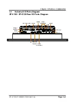
Page 25: ...xternal I O Ports Diagram SP 6150 SP 6155 Rear I O Ports Diagram SS SS SS Remote SW RESET DC IN 9 36V COM2 GND VCC DVI D HDMI I2 C COM1 LAN1 LAN2 PoE ON 1 2 DC IN 9 36V DVI D HDMI USB Connector LAN1 L...

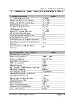
Page 26: ...DS Panel On Off Sequence Selection JP10 LVDS Panel Inverter 12V Soft Start Time Selection JP10 Slide Switch for LVDS Resolution Selection SW2 System CONNECTOR Description NAME Rear I O Port Connectors...

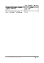
Page 27: ...e Configuration SP 6150 6155 SERIES USER MANUAL Page 3 4 System CONNECTOR Description NAME HDD Power Connector SATA_PWR1 I2C Wafer JI2C1 JI2C2 Low Pin Count LPC Connector JLPC1 Power over Ethernet PoE...

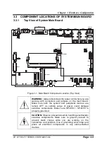
Page 28: ...ge while you are working on the connectors and jumpers Use a grounding wrist strap and place all electronic components in any static shielded devices JP_VDD1 3 1 JP7 20 19 1 1 30 29 2 1 2 1 2 3 LVDS1...

Page 29: ...R MANUAL Page 3 6 CAUTION Always touch the motherboard components by the edges Never touch components such as a processor by its pins Take special cares while you are holding electronic circuit boards...

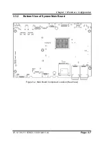
Page 30: ...Chapter 3 Hardware Configuration SP 6150 6155 SERIES USER MANUAL Page 3 7 3 3 2 Bottom View of System Main Board Figure 3 2 Main Board Component Location Rear View...

Page 31: ...ngs by opening or closing jumpers Jumpers can be combined into sets that are called jumper blocks When jumpers are all in the block you have to put them together to set up the hardware configuration T...

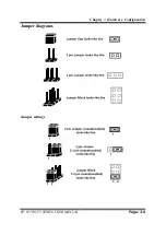
Page 32: ...Chapter 3 Hardware Configuration SP 6150 6155 SERIES USER MANUAL Page 3 9 Jumper diagrams Jumper settings...

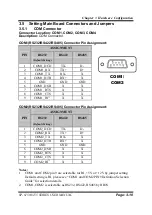
Page 33: ...RX X 5 GND GND GND 6 COM1_DSR X X 7 COM1_RTS X X 8 COM1_CTS X X 9 COM1_RI 1 X X COM2 RS232 RS422 RS485 Connector Pin Assignment PIN ASSIGNMENT RS232 Default Setting RS422 RS485 1 COM2_DCD TX D 2 COM2...

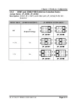
Page 34: ...5 2 COM1 and COM2 PIN9 Definition Selection Guide Jumper Name JP_COM1 JP_COM2 Description COM1 JP_COM1 and COM2 pin9 JP_COM2 RI 5V 12V Selection SELECTION JUMPER SETTING JUMPER ILLUSTRATION RI 1 2 De...

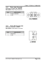
Page 35: ...12 3 5 3 Power Input Connector Connector Location CN_POWER1 Description Power Input Connector PIN ASSIGNMENT 1 WIDE_POWERIN 2 GND 3 5 4 Power Button Connector Connector Location J_PBTN1 Description P...

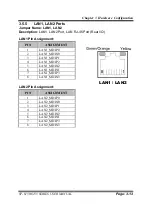
Page 36: ...n LAN1 LAN2 Port LAN RJ 45 Port Rear I O LAN1 Pin Assignment PIN ASSIGNMENT 1 LAN1_MDIP0 2 LAN1_MDIN0 3 LAN1_MDIP1 4 LAN1_MDIP2 5 LAN1_MDIN2 6 LAN1_MDIN1 7 LAN1_MDIP3 8 LAN1_MDIN3 LAN2 Pin Assignment...

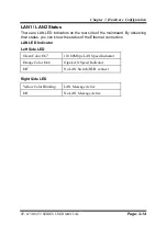
Page 37: ...side of the mainboard By observing their status you can know the status of the Ethernet connection LAN LED Indicator Left Side LED Green Color On7 10 100Mbps LAN Speed Indicator Orange Color On8 Giga...

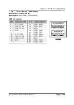
Page 38: ...Location USB1 Description Dual USB 3 0 Connectors USB 3 0 signals PIN ASSIGNMENT PIN ASSIGNMENT A1 VCC5_USB1 A5 USB3_RXN1 A2 USB2_P1_DN A6 USB3_RXP1 A3 USB2_P1_DP A7 GND A4 GND A8 USB3_TXN1 A9 USB3_TX...

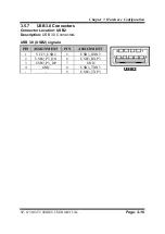
Page 39: ...SER MANUAL Page 3 16 3 5 7 USB 3 0 Connectors Connector Location USB2 Description USB 3 0 Connectors USB 3 0 USB2 signals PIN ASSIGNMENT PIN ASSIGNMENT 1 VCC5_USB2 5 USB3_RXN3 2 USB2_P3_DN 6 USB3_RXP3...

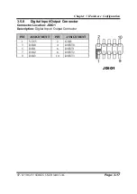
Page 40: ...SERIES USER MANUAL Page 3 17 3 5 8 Digital Input Output Connector Connector Location JDIO1 Description Digital Input Output Connector PIN ASSIGNMENT PIN ASSIGNMENT 1 VCC5 2 GND 3 DIN0 4 DOUT0 5 DIN1...

Page 41: ...UAL Page 3 18 3 5 9 I2C Wafer Connector Location JI2C1 JI2C2 Description I2C Wafer JI2C1 Pin Assignment PIN ASSIGNMENT 1 GND 2 V3P3S VCC5 3 I2C4_SCL_33 4 I2C4_SDA_33 JI2C2 Pin Assignment PIN ASSIGNMEN...

Page 42: ...voltage of JI2C1 and JI2C2 SELECTION JUMPER SETTING JUMPER ILLUSTRATION JI2C1 pin2 3 3V 1 3 Default Setting JP_I2C1 JI2C1 pin2 5V 3 5 JP_I2C1 JI2C2 pin2 3 3V 2 4 Default Setting JP_I2C1 JI2C2 pin2 5V...

Page 43: ...on DVI Digital Visual Interface Connector PIN ASSIGNMENT PIN ASSIGNMENT 1 DP0_DVI_N2 13 NC 2 DP0_DVI_P2 14 VCC5_DVI 3 GND 15 CRT_CLK 4 NC 16 DP0_DVI_HPD_IN 5 NC 17 DP0_DVI_N0 6 DP0_DVI_SCL 18 DP0_DVI_...

Page 44: ...2 Description Display Port Connector HDMI Connector HDMI1 signals PIN ASSIGNMENT PIN ASSIGNMENT 1 DP1_HDMI_P2 2 GND 3 DP1_HDMI_N2 4 DP1_HDMI_P1 5 GND 6 DP1_HDMI_N1 7 DP1_HDMI_P0 8 GND 9 DP1_HDMI_N0 10...

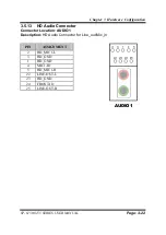
Page 45: ...S USER MANUAL Page 3 22 3 5 13 HD Audio Connector Connector Location AUDIO1 Description HD Audio Connector for Line_out Mic_in PIN ASSIGNMENT 2 HD_MIC1 L 3 HD_GND 1 HD_GND 4 MIC1 JD 5 HD_MIC1 R 22 LIN...

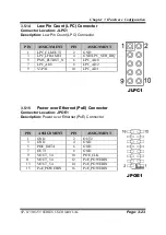
Page 46: ...Connector Location JPOE1 Description Power over Ethernet PoE Connector PIN ASSIGNMENT PIN ASSIGNMENT 1 LPC_CLKOUT1 2 GND 3 LPC_LFRAMEJ 4 GND LPC_SER_IRQ 5 PMU_PLTRST_N 6 LPC_AD0 7 LPC_AD3 8 LPC_AD2 9...

Page 47: ...GND 19 SIM1_SW1 20 NC 21 GND 22 PMU_PLTRST_N 23 PCIE_P2_RXN 24 V3_3A 25 PCIE_P2_RXP 26 GND 27 GND 28 V1P5S_MINI 29 GND 30 SMB_3P3_SCL 31 PCIE_P2_TXN 32 SMB_3P3_SDA 33 PCIE_P2_TXP 34 GND 35 GND 36 USB...

Page 48: ...MENT 1 LVDS_VCC 2 GND 3 LVDS_CLKB_DN 4 LVDS_CLKB_DP 5 GND 6 LVDS_B2_DN 7 LVDS_B2_DP 8 GND 9 LVDS_B1_DN 10 LVDS_B1_DP 11 LVDS_B3_DP 12 LVDS_B3_DN 13 LVDS_B0_DP 14 LVDS_B0_DN 15 GND 16 LVDS_CLKA_DP 17 L...

Page 49: ...tor Location JINV1 Description Panel Inverter Connector PIN ASSIGNMENT PIN ASSIGNMENT 1 V5P0A 2 V5P0A 3 USB2_P5_DN 4 V12P0_INV 5 USB2_P5_DP 6 V12P0_INV 7 GND 8 V12P0_INV 9 LVDS_BKLTEN 10 V12P0_INV 11...

Page 50: ...ND 5 NC 6 NC 7 NC 8 SIM2_PWR 9 GND 10 SIM2_DATA 11 NC 12 SIM2_CLK 13 NC 14 SIM2_RESET 15 GND 16 SIM2_VPP 17 SIM2_SW2 18 GND 19 SIM2_SW1 20 NC 21 GND 22 NC 23 SATA_RXP1 24 V3P3S_MSATA 25 SATA_RXN1 26 G...

Page 51: ...A 3 0 Connector Connector Location SATA1 Description Serial ATA SATA 3 0 Connector 3 5 21 HDD Power Connector Connector Location SATA_PWR1 Description HDD Power Connector PIN ASSIGNMENT 1 VCC5 2 GND P...

Page 52: ...JP_ATX1 Description AT ATX Mode Selection SELECTION JUMPER SETTING JUMPER ILLUSTRATION ATX Open Default Setting JP_ATX1 AT 1 2 JP_ATX1 3 5 23 TPM Module Selection Connector Location JP_TPM1 Descripti...

Page 53: ...h for LVDS Resolution Channel Color Bit Selection SELECTION SW2 PIN SETTING 800 x 600 1CH 18bit 1 ON 2 ON 3 ON 4 ON 1024 x 768 1CH 18bit 1 OFF 2 ON 3 ON 4 ON 1024 x 768 1CH 24bit SP 7155 Default Setti...

Page 54: ...1 OFF 2 ON 3 OFF 4 ON 1280 x 1024 2CH 24bit SP 7157 Default Setting 1 ON 2 OFF 3 OFF 4 ON 1366 x 768 1CH 18bit 1 OFF 2 OFF 3 OFF 4 ON 1366 x 768 1CH 24bit 1 ON 2 ON 3 ON 4 OFF 1440 x 900 2CH 24bit 1 O...

Page 55: ...SETTING 4 OFF 1600 x 900 2CH 24bit 1 OFF 2 OFF 3 ON 4 OFF 1680 x 1050 2CH 24bit 1 ON 2 ON 3 OFF 4 OFF 1600 x 1200 2CH 24bit 1 OFF 2 ON 3 OFF 4 OFF 1920 x 1080 2CH 24bit 1 ON 2 OFF 3 OFF 4 OFF 1920 x 1...

Page 56: ...S USER MANUAL Page 3 33 3 5 25 LVDS Display Selection Connector Location JP_EDP1 JP7 Description Display selection to LVDS by JP_EDP1 and JP7 SELECTION JUMPER SETTING JUMPER ILLUSTRATION LVDS 2 3 Defa...

Page 57: ...onnector Location JP_VDD1 Description Voltage selection jumper for selecting PIN1 PIN29 PIN30 LVDS_VCC voltage of LVDS1 SELECTION JUMPER SETTING JUMPER ILLUSTRATION 3 3V 1 2 Default Setting JP_VDD1 5V...

Page 58: ...Location JP6 Description Jumper for selecting PIN18 LVDS_BKLCTL voltage of JINV1 SELECTION JUMPER SETTING JUMPER ILLUSTRATION 3 3V 1 2 Default Setting JP6 5V 2 3 JP6 Note 1 Users can change the settin...

Page 59: ...iption Set pins 1 3 and 2 4 as connected for controlling LVDS Panel On Off Sequence by CPU Set pins 3 5 and 4 6 as connected for controlling LVDS Panel On Off Sequence by CH7511 SELECTION JUMPER SETTI...

Page 60: ...verter 12V Soft Start Time Selection Connector Location JP10 Description LVDS Panel Inverter 12V Soft Start Time Selection SELECTION JUMPER SETTING JUMPER ILLUSTRATION 2ms Open Default Setting JP10 20...

Page 61: ...PC Step2 Close JP4 pins 1 2 for 6 seconds by a cap Step3 Remove the cap which is just used on JP4 1 2 so that JP4 returns to OPEN Step4 Power on the PC and the PC will then auto reboot for once in ord...

Page 62: ...55 SERIES USER MANUAL Page 3 39 3 5 31 MicroSD Card Connector Connector Location SDCARD1 rear side of mainboard Description MicroSD Secure Digital Card Connector PIN ASSIGNMENT 1 DAT3 2 CMD 3 GND 4 VD...

Page 63: ...6155 SERIES USER MANUAL Page 3 40 3 5 32 SIM Card Connectors Connector Location SIM1 SIM2 rear side of mainboard Description SIM Subscriber Identity Module Card Connectors PIN ASSIGNMENT C1 VCC C2 RS...

Page 64: ...anel Low Signal Setting JP2 CONNECTOR Description NAME Control Signal Connector SGN_BRD1 LVDS Panel Signal Connector Connected To Motherboard LVDS_MB1 LVDS Panel Signal Connector Connected To LCD Pane...

Page 65: ...NECTORS AND JUMPERS 3 8 1 Control Signal Connector Connector Location SGN_BRD1 Description Control Signal Connector PIN ASSIGNMENT PIN ASSIGNMENT 1 5VSB 2 5VSB 3 USB D 4 12V 5 USB D 6 12V 7 GND 8 12V...

Page 66: ...GNMENT 1 LVDS_VCC 2 GND 3 LVDS1_CLK Even 4 LVDS1_CLK Even 5 GND 6 LVDS1_D2 Even 7 LVDS1_D2 Even 8 GND 9 LVDS1_D1 Even 10 LVDS1_D1 Even 11 LVDS1_D3 Even 12 LVDS1_D3 Even 13 LVDS1_D0 Even 14 LVDS1_D0 Ev...

Page 67: ...NMENT 1 LVDS_VCC 2 GND 3 LVDS1_CLK Even 4 LVDS1_CLK Even 5 GND 6 LVDS1_D2 Even 7 LVDS1_D2 Even 8 GND 9 LVDS1_D1 Even 10 LVDS1_D1 Even 11 LVDS1_D3 Even 12 LVDS1_D3 Even 13 LVDS1_D0 Even 14 LVDS1_D0 Eve...

Page 68: ...cation JLED_DRV Description 15 Panel LED Backlight Control Connector 3 8 5 Touch Panel Connector Connector Location JTP1 Description Touch Panel Connector PIN ASSIGNMENT 1 12V 2 12V 3 GND 4 LCD_PWM PI...

Page 69: ...Chapter 3 Hardware Configuration SP 6150 6155 SERIES USER MANUAL Page 3 46 3 8 6 LED1 Connector Connector Location JLED1 Description LED1 Connector PIN ASSIGNMENT 1 VCC 2 POWER LED 3 HDD LED JLED1...

Page 70: ...ting Jumper Name JP1 Description Touch Panel Up Signal Setting SELECTION JUMPTER SETTING JUMPER ILLUSTRATION Normal Open Default Setting JP1 Connect Up Left Signal 1 2 JP1 Connect Up Right Signal 5 6...

Page 71: ...ng Jumper Name JP2 Description Touch Panel Low Signal Setting SELECTION JUMPTER SETTING JUMPER ILLUSTRATION Normal Open Default Setting JP2 Connect Low Left Signal 1 2 JP2 Connect Low Right Signal 5 6...

Page 72: ...e system The following topics are included Installing Intel Chipset Software Installation Utility Installing Intel Trusted Execution Engine Driver installation Microsoft Hotfix kb3211320 and kb3213986...

Page 73: ...atform Main Chip Intel Chipset Device Software Installation Utility X D Driver Platform Graphics Intel N3350 For VGA Driver installation X D Driver Platform Hotfix Microsoft Hotfix kb3211320 and kb321...

Page 74: ...Support Identification of Intel Chipset Components in the Device Manager 4 2 2 Intel Chipset Software Installation Utility The utility pack is to be installed only for Windows 10 series and it should...

Page 75: ...pend on the system s specific hardware and firmware features The installer compatible with Windows 10 detects the system s capabilities and installs the relevant drivers and applications 4 3 2 Install...

Page 76: ...ystem s specific hardware and firmware features The installer compatible with Windows 10 detects the system s capabilities and installs the relevant drivers and applications 4 4 2 Installation Instruc...

Page 77: ...e system work simultaneously To install the Graphics driver utility follow the steps below 1 Connect the USB DVD ROM device to SP 6150 SP 6155 and insert the driver disk 2 Enter the Graphics folder wh...

Page 78: ...device to SP 6150 SP 6155 and insert the driver disk 2 Enter the LAN Chip folder where the driver is located 3 Click Autorun exe file for driver installation 4 Follow the on screen instructions to com...

Page 79: ...the steps below 1 Connect the USB DVD ROM device to SP 6150 SP 6155 and insert the driver disk 2 Open the Sound Codec folder where the driver is located 3 Click the Audio_0008 64bit_Win7_Win8_Win81_W...

Page 80: ...device to SP 6150 SP 6155 and insert the driver disk 2 Open the Serial I O folder where the driver is located 3 Select Windows 10 64 bit for your OS platform 4 Click the SetupSerialIO exe file for dri...

Page 81: ...tup Utilities The information of the system configuration is saved in battery backed CMOS RAM and BIOS NVRAM so that the Setup information is retained when the system is powered off The BIOS Setup Uti...

Page 82: ...EFI Unified Extensible Firmware Interface specifications and the Intel Platform Innovation Framework for EFI The UEFI specification defines an interface between the operating system and platform firmw...

Page 83: ...venient for engineers to perform modifications and customize the computer system and allows technicians to troubleshoot the occurred errors when the hardware is faulty The BIOS setup menu allows users...

Page 84: ...fter the system is powered on BIOS will enter the Power On Self Test POST routines and the POST message will be displayed Figure 5 2 POST Screen with AMI Logo Press Del or Esc to access the Setup Util...

Page 85: ...item a brief description of the highlighted selection will appear on the right side of the screen The language of the BIOS setup menu interface and help messages are shown in US English You may use o...

Page 86: ...BIOS setup menu BIOS Messages This section describes the alert messages generated by the board s BIOS These messages would be shown on the monitor when certain recoverable errors events occur during...

Page 87: ...and Time Main Screen BIOS Setting Options Description Purpose BIOS Vendor No changeable options Displays the name of the BIOS vendor Core Version No changeable options Displays the current BIOS core v...

Page 88: ...r Sets the system date The format is Day Month Date Year Users can directly enter values or use or arrow keys to increase decrease it The Day is automatically changed System Time hour minute second Se...

Page 89: ...Advanced Menu Screen BIOS Setting Options Description Purpose ACPI Settings Sub Menu System ACPI Parameters Hardware Monitor Sub Menu Monitor hardware status F81946 Watchdog Sub Menu F81946 Watchdog...

Page 90: ...State ACPI Settings Screen BIOS Setting Options Description Purpose Enable Hibernation Disabled Enabled Enables or Disables System ability to Hibernate OS S4 Sleep State This option may be not effect...

Page 91: ...cessor s temperature System Temperature No changeable options Displays the system s temperature VCORE No changeable options Detects and displays the VCORE CPU voltage VCC5V No changeable options Detec...

Page 92: ...trigger a system reset via the 255 level watchdog timer F81946 Watchdog Configuration Screen BIOS Setting Options Description Purpose Enable Watchdog Enabled Disabled Enables Disables F81946 Watchdog...

Page 93: ...ion Purpose Socket 0 CPU Information Sub menu Socket specific CPU Information CPU Power Management Sub menu CPU Power Management options Intel Virtualization Technology Disabled Enabled When enabled a...

Page 94: ...CPU Microcode Patch Revision Max CPU Speed No changeable options Displays the maximum CPU speed Min CPU Speed No changeable options Displays the minimum CPU speed Processor Cores No changeable options...

Page 95: ...chnology VT a VMM Virtual Machine Monitor can utilize the additional hardware capabilities L1 Data Cache No changeable options Displays L1 Data Cache Size L1 Code Cache No changeable options Displays...

Page 96: ...Page 5 16 5 4 4 2 Advanced CPU Configuration CPU Power Management Menu Path Advanced CPU Configuration CPU Power Management CPU Power Management Screen BIOS Setting Options Description Purpose EIST D...

Page 97: ...nfiguration Menu Path Advanced F81946 Super IO Configuration F81946 Super IO Configuration Screen BIOS Setting Options Description Purpose Serial Port 1 Configuration Sub menu Sets the parameters of S...

Page 98: ...rpose Serial Port Disabled Enabled Enables or Disables Serial Port 1 Device settings No changeable options Displays the current settings of Serial Port 1 Change Settings Auto IO 3F8h IRQ 4 IO 3F8h IRQ...

Page 99: ...rpose Serial Port Disabled Enabled Enables or Disables Serial Port 2 Device Settings No changeable options Displays the current settings of Serial Port 2 Change Settings Auto IO 2F8h IRQ 6 IO 3F8h IRQ...

Page 100: ...to the LAN via a jumper which keeps the workstation connected to the network even when the power is turned off Network Stack Configuration Screen BIOS Setting Options Description Purpose Network Stac...

Page 101: ...Advanced USB Configuration The USB Configuration allows users to configure advanced USB settings such as USB mass storage driver support USB Configuration Screen BIOS Setting Options Description Purp...

Page 102: ...Menu Path Advanced Platform Trust Technology The Platform Trust Technology allows users to configure advanced TPM settings such as fTPM Platform Trust Technology Screen BIOS Setting Options Descripti...

Page 103: ...h Chipset This menu allows users to configure advanced Chipset settings such as North Bridge and South Bridge configuration parameters Chipset Screen BIOS Setting Options Description Purpose North Bri...

Page 104: ...u Path Chipset North Bridge North Bridge Screen BIOS Setting Options Description Purpose Total Memory No changeable options Displays the current amount and type of memory on the system e g 2048 MB SO...

Page 105: ...ng Options Description Purpose HD Audio Configuration Sub menu HD Audio Configuration Settings LPSS Configuration Sub menu LPSS Configuration Settings PCI Express Configuration Sub menu PCI Express Co...

Page 106: ...5 26 5 5 2 1 Chipset South Bridge HD Audio Configuration Menu Path Chipset South Bridge HD Audio Configuration HD Audio Configuration Screen BIOS Setting Options Description Purpose HD Audio Configura...

Page 107: ...Configuration Screen BIOS Setting Options Description Purpose I2C1 Support Disabled Enabled Enables or Disables I2C1 Support Set I2C1 Speed Standard Mode Fast Mode Fast Plus Mode High Speed Mode Selec...

Page 108: ...Bridge PCI Express Configuration PCI Express Configuration Screen BIOS Setting Options Description Purpose PCI Express Root Port 0 LAN 1 Sub menu PCI Express Root Port 0 LAN 1 parameters PCI Express...

Page 109: ...ot Port 0 LAN 1 Configuration Screen BIOS Setting Options Description Purpose PCI Express Root Port 0 LAN 1 Disabled Enabled Auto default Enables or Disables PCI Express Root Port 0 LAN 1 AUTO Disable...

Page 110: ...ot Port 1 LAN 2 Configuration Screen BIOS Setting Options Description Purpose PCI Express Root Port 1 LAN 2 Disabled Enabled Auto default Enables or Disables PCI Express Root Port 0 LAN 1 AUTO Disable...

Page 111: ...PCI Express Port 1 Disabled Enabled Auto default Enables or Disables the Mini PCI Express Root Port 1 AUTO Disables the unused Root Port automatically for saving the most optimum power Enabled Enables...

Page 112: ...Setup SP 6150 6155 SERIES USER MANUAL Page 5 32 BIOS Setting Options Description Purpose Hot Plug Disabled Enabled Enables or Disables PCI Express Hot Plug PCIe Speed Auto Gen1 Gen2 Selects PCI Expre...

Page 113: ...Options Description Purpose Chipset SATA Disabled Enabled Enables or Disables the Chipset SATA Controller SATA Port 1 No changeable options Displays the connected device on SATA Port 1 Port 1 Disabled...

Page 114: ...laneous Configuration Screen BIOS Setting Options Description Purpose State After G3 S0 State S5 State Specify what state to go to when power is re applied after power failure G3 state S0 State System...

Page 115: ...s from changing your BIOS settings You can configure an Administrator password and then configure a user password An administrator has much more privileges over the settings in the Setup utility than...

Page 116: ...rd User Password option from the Security menu and press Enter and the password dialog entry box appears 2 Select the Administrator Password or User Password that you want to change A password can be...

Page 117: ...anging the boot order from the available bootable device s Boot Screen BIOS Setting Options Description Purpose Setup Prompt Timeout Numeric from 1 to 65535 Number of seconds to wait for setup activat...

Page 118: ...OS will display normal POST messages Fast Boot Disabled Enabled Enables or Disables Fast Boot option It allows users to reduce the system startup time and start up the system in a fast manner Boot Opt...

Page 119: ...the changes and then exit the system Select Save Changes and Reset to validate the changed BIOS settings and then restart the system Discard Changed BIOS Settings To cancel the BIOS settings you have...

Page 120: ...et No changeable options Resets the system without saving any changes configured in BIOS settings Save Changes No changeable options Saves the changes done so far to any of the setup options Discard C...

Page 121: ...el Exploded Diagram SP 6150 Touch Control Board Exploded Diagram SP 6150 Box Exploded Diagram SP 6155 Touch Panel Exploded Diagram SP 6155 LCD Display Exploded Diagram SP 6155 Panel Mount Exploded Dia...

Page 122: ...5311 4 4 Flat Head Screw M3x0 5Px6mm Black 22 215 30060011 2 5 LED Housing Black 30 014 04100165 2 6 LED Holder 20 029 03003130 1 7 Panel Bracket Standard L 20 006 03001130 1 8 Power HDD LED Cable L 2...

Page 123: ...03001239 2 23 Touch Support TB 20 006 03002239 2 24 Poron Sponge 175x11 6x0 5mm 90 013 24100000 2 25 Poron Sponge 233x11 6x0 5mm 90 013 24200000 2 26 10 4 ELO Touch Panel 5 Wire Resistive 52 380 01510...

Page 124: ...SP 6150 6155 SERIES USER MANUAL Page A 4 SP 6150 Front Panel Exploded Diagram No Component Name P N No Q ty 1 Flat Head Screw M3x0 5Px6mm Black 22 215 30060011 8 2 CPT LCD Assembly 1 3 Front Panel As...

Page 125: ...155 SERIES USER MANUAL Page A 5 SP 6150 Touch Control Board Exploded Diagram 01 02 03 No Component Name P N No Q ty 1 Round Washer Head Screw M3x0 5Px5mm 22 242 30005311 4 2 PAC8100LF D1 PCB SR 6145RA...

Page 126: ...grams SP 6150 6155 SERIES USER MANUAL Page A 6 SP 6150 Box Exploded Diagram No Component Name Part No Q ty 1 Outside Rubber 30 013 01100239 1 2 SE 8134 1 3 Flat Head Screw M3x0 5Px6mm Black 22 215 300...

Page 127: ...RIES USER MANUAL Page A 7 SP 6155 Touch Panel Exploded Diagram No Component Name Part No Q ty 1 SP 6155_LCD_Module_Exp See page A 8 1 2 SE 8134 Explode See page A 11 A 15 1 3 Flat Head Screw 2 5 M3x0...

Page 128: ...002417 2 5 SP 6155 LED Support 20 002 03001417 1 6 15 5 wire Resistance AccuTouch Panel 52 351 03650511 1 7 15 TFT LCD Panel LED Backlight 450nits HD 1024x768 52 351 03006802 1 8 SP 6205 Touch Panel E...

Page 129: ...SP 6145 Wall Waterproof Rubber 90 013 01100351 1 15 Flat Label For Porx 34 017 02104009 1 16 PPC 7360 LED Label For Power 34 017 02103009 1 17 LED Label For HDD 34 017 02101009 1 18 Round Head With S...

Page 130: ...Appendix A System Diagrams SP 6150 6155 SERIES USER MANUAL Page A 10 SP 6155 Panel Mount Exploded Diagram...

Page 131: ...SP 6150 SP 6155 Button Cover Exploded Diagram No Component Name P N No Q ty 1 SP 6155 SE 8134 PPC Bottom Bracket w Paint Black 80 006 03061417 1 2 Flat Head Screw 2 M3x0 5Px5mm Black 22 215 30005011 5...

Page 132: ...1 002 24525001 1 N3350 81 002 24525002 4 Choke Thermal Pads K 12 15x15x1 0mm Gray 81 006 81515007 1 5 CPU Thermal Pads K 12 13x13x1mm Gray 81 006 81313003 1 6 Flat Head Screw M3 4 0 5 0kg cm 22 215 30...

Page 133: ...mponent Name P N No Q ty 1 Heat Sink Left Cover Black 81 002 11841003 1 Silver 81 002 11841004 2 SB 8134 M B 1 3 PoE Board SR 8134RB D0N 1 4 HEX CU BOSS NI M3x0 5Px6L H 24 7mm 22 252 30025901 4 5 Fill...

Page 134: ...03062401 3 SIM SD Cover Blue 20 004 03063401 1 Silver 20 004 03064401 4 COM Port Cable 27 024 40105031 2 27 024 40107031 5 I 2 C Cable 27 067 4010 5071 1 6 Remote SW Cable 27 055 40102071 1 7 LED Hou...

Page 135: ...4 HDD Cable Holder ASM 20 029 03001401 1 4 SE 8134 HDD Support Bracket 20 006 03001401 1 5 HDD Cable 27 008 40103081 1 6 Flat Head Screw 2 M3x0 5Px5mm Black 22 215 30005011 4 7 Fillister Head Screw 2...

Page 136: ...SP 6140 EPE LEFT 325x180x112mm 94 016 00302347 1 8 Accessories Box 234X155X45mm for PS8830X with Compact Stand 34 003 01301026 1 9 Outer Carton 382x185x338mm 34 003 01301088 1 Accessories Box 234X155...

Page 137: ...Boxes 332x150x45mm 34 003 01301086 1 4 PE Bag 480x460 32 100 20010000 1 5 Silica Gel 1gm 34 005 00010007 2 6 SP 6155 System N A 1 DVD R w Protech logo For OBM 52 601 02000005 1 Mylar 335x260x0 125 30...

Page 138: ...B Technical Summary This appendix will give you a brief introduction of the allocation maps for the system resources The following topics are included System Block Diagram Interrupt Map I O Map Memory...

Page 139: ...ini PCI E Slot SIM SD CARD COM 1 2 RS232 422 485 COM1 2 support 5V 12V F81964D I Super IO RS 232 LOW PIN COUNT SDMMC SMBUS DDR3L X 1 DDR3L 8GB CH7511 LVDS DP to LVDS LVDS Connector eDP non ECC SODIMM...

Page 140: ...System IRQ 55 Microsoft ACPI Compliant System IRQ 56 Microsoft ACPI Compliant System IRQ 57 Microsoft ACPI Compliant System IRQ 58 Microsoft ACPI Compliant System IRQ 59 Microsoft ACPI Compliant Syst...

Page 141: ...84 Microsoft ACPI Compliant System IRQ 85 Microsoft ACPI Compliant System IRQ 86 Microsoft ACPI Compliant System IRQ 87 Microsoft ACPI Compliant System IRQ 88 Microsoft ACPI Compliant System IRQ 89 M...

Page 142: ...15 Microsoft ACPI Compliant System IRQ 116 Microsoft ACPI Compliant System IRQ 117 Microsoft ACPI Compliant System IRQ 118 Microsoft ACPI Compliant System IRQ 119 Microsoft ACPI Compliant System IRQ 1...

Page 143: ...46 Microsoft ACPI Compliant System IRQ 147 Microsoft ACPI Compliant System IRQ 148 Microsoft ACPI Compliant System IRQ 149 Microsoft ACPI Compliant System IRQ 150 Microsoft ACPI Compliant System IRQ 1...

Page 144: ...77 Microsoft ACPI Compliant System IRQ 178 Microsoft ACPI Compliant System IRQ 179 Microsoft ACPI Compliant System IRQ 180 Microsoft ACPI Compliant System IRQ 181 Microsoft ACPI Compliant System IRQ 1...

Page 145: ...59 Microsoft ACPI Compliant System IRQ 260 Microsoft ACPI Compliant System IRQ 261 Microsoft ACPI Compliant System IRQ 262 Microsoft ACPI Compliant System IRQ 263 Microsoft ACPI Compliant System IRQ 2...

Page 146: ...90 Microsoft ACPI Compliant System IRQ 291 Microsoft ACPI Compliant System IRQ 292 Microsoft ACPI Compliant System IRQ 293 Microsoft ACPI Compliant System IRQ 294 Microsoft ACPI Compliant System IRQ 2...

Page 147: ...321 Microsoft ACPI Compliant System IRQ 322 Microsoft ACPI Compliant System IRQ 323 Microsoft ACPI Compliant System IRQ 324 Microsoft ACPI Compliant System IRQ 325 Microsoft ACPI Compliant System IRQ...

Page 148: ...352 Microsoft ACPI Compliant System IRQ 353 Microsoft ACPI Compliant System IRQ 354 Microsoft ACPI Compliant System IRQ 355 Microsoft ACPI Compliant System IRQ 356 Microsoft ACPI Compliant System IRQ...

Page 149: ...383 Microsoft ACPI Compliant System IRQ 384 Microsoft ACPI Compliant System IRQ 385 Microsoft ACPI Compliant System IRQ 386 Microsoft ACPI Compliant System IRQ 387 Microsoft ACPI Compliant System IRQ...

Page 150: ...414 Microsoft ACPI Compliant System IRQ 415 Microsoft ACPI Compliant System IRQ 416 Microsoft ACPI Compliant System IRQ 417 Microsoft ACPI Compliant System IRQ 418 Microsoft ACPI Compliant System IRQ...

Page 151: ...445 Microsoft ACPI Compliant System IRQ 446 Microsoft ACPI Compliant System IRQ 447 Microsoft ACPI Compliant System IRQ 448 Microsoft ACPI Compliant System IRQ 449 Microsoft ACPI Compliant System IRQ...

Page 152: ...476 Microsoft ACPI Compliant System IRQ 477 Microsoft ACPI Compliant System IRQ 478 Microsoft ACPI Compliant System IRQ 479 Microsoft ACPI Compliant System IRQ 480 Microsoft ACPI Compliant System IRQ...

Page 153: ...ft ACPI Compliant System IRQ 510 Microsoft ACPI Compliant System IRQ 511 Microsoft ACPI Compliant System IRQ 1024 Intel SD Host Controller IRQ 4294967277 Intel R HD Graphics IRQ 4294967278 Intel R I21...

Page 154: ...eXtensible Host Controller 1 0 Microsoft IRQ 4294967291 Intel R Trusted Execution Engine Interface IRQ 4294967292 Standard SATAAHCI Controller IRQ 4294967293 Intel R Celeron R Pentium R Processor PCI...

Page 155: ...0070 0x00000070 System CMOS real time clock 0x00000080 0x0000008F Motherboard resources 0x00000092 0x00000092 Motherboard resources 0x000000B2 0x000000B3 Motherboard resources 0x00000680 0x0000069F Mo...

Page 156: ...ammable interrupt controller 0x0000003C 0x0000003D Programmable interrupt controller 0x000000A0 0x000000A1 Programmable interrupt controller 0x000000A4 0x000000A5 Programmable interrupt controller 0x0...

Page 157: ...rces 0xFEE00000 0xFEEFFFFF Motherboard resources 0x91310000 0x91313FFF High Definition Audio Controller 0x91000000 0x910FFFFF High Definition Audio Controller 0x91316000 0x913160FF Intel R Celeron R P...

Page 158: ...er 5AB6 0x7C000001 0x7FFFFFFF PCI Express Root Complex 0x7B800001 0x7BFFFFFF PCI Express Root Complex 0x91321000 0x91321FFF Intel R Trusted Execution Engine Interface 0xD0C00000 0xD0C00653 Intel R Ser...

Page 159: ...igure the configuration registers The chip selects the Logical Device and activates the desired Logical Devices through Extended Function Index Register EFIR and Extended Function Data Register EFDR T...

Page 160: ...xtended function mode mov dx 2eh mov al 87h out dx al out dx al Select Logical Device 7 of watchdog timer mov al 07h out dx al inc dx mov al 07h out dx al Enable Watch dog feature mov al 030h out dx a...

Page 161: ...150 6155 SERIES USER MANUAL Page B 24 mov al 1Eh out dx al Set second as counting unit and start counting dec dx mov al 0F5h out dx al inc dx in al dx and al 30h out dx al Exit the extended function m...

Page 162: ...sh utility AFUEFIx64 exe v5 09 01 into the storage device The utility and BIOS file should be saved to the same path 4 Make sure the target system can first boot to the EFI shell environment 1 Connect...

Page 163: ...ID II BIOS Update Procedure 1 Use the bootable USB storage to boot up the system into the DOS command prompt Shell fs0 fs0 cd afuefix64 2 Type AFUEFIx64 615Xxxxx bin p b n x and press Enter to start t...

Page 164: ...RomLayout Ok Erasing Boot Block done Updating Boot Block done Verifying Boot Block done Erasing Main Block done Updating Main Block done Verifying Main Block done Erasing NVRAM Block done Updating NVR...

Reviews: